
SN74AHCT1G14 Single Schmitt-Trigger Inverter
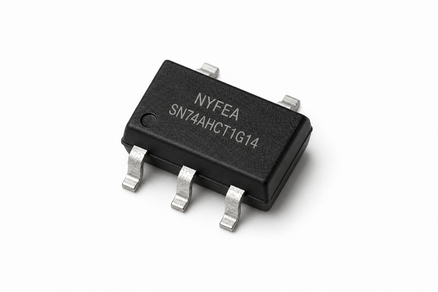
NYFEA SN74AHCT1G14 is a single positive-logic inverter with a Schmitt-trigger input, a 2.0 V to 5.5 V recommended supply range, TTL-compatible input behavior and partial-power-down support through Ioff.
Product scope: This device conditions one digital input and produces the inverted logic state. Separate positive-going and negative-going thresholds provide hysteresis for slow or noisy signals; it is not an analog comparator, oscillator, level translator or power driver.
Use the current controlled PDF for threshold limits, switching conditions, package tolerances, tape orientation and production-release decisions.
Product Overview and Selection Scope
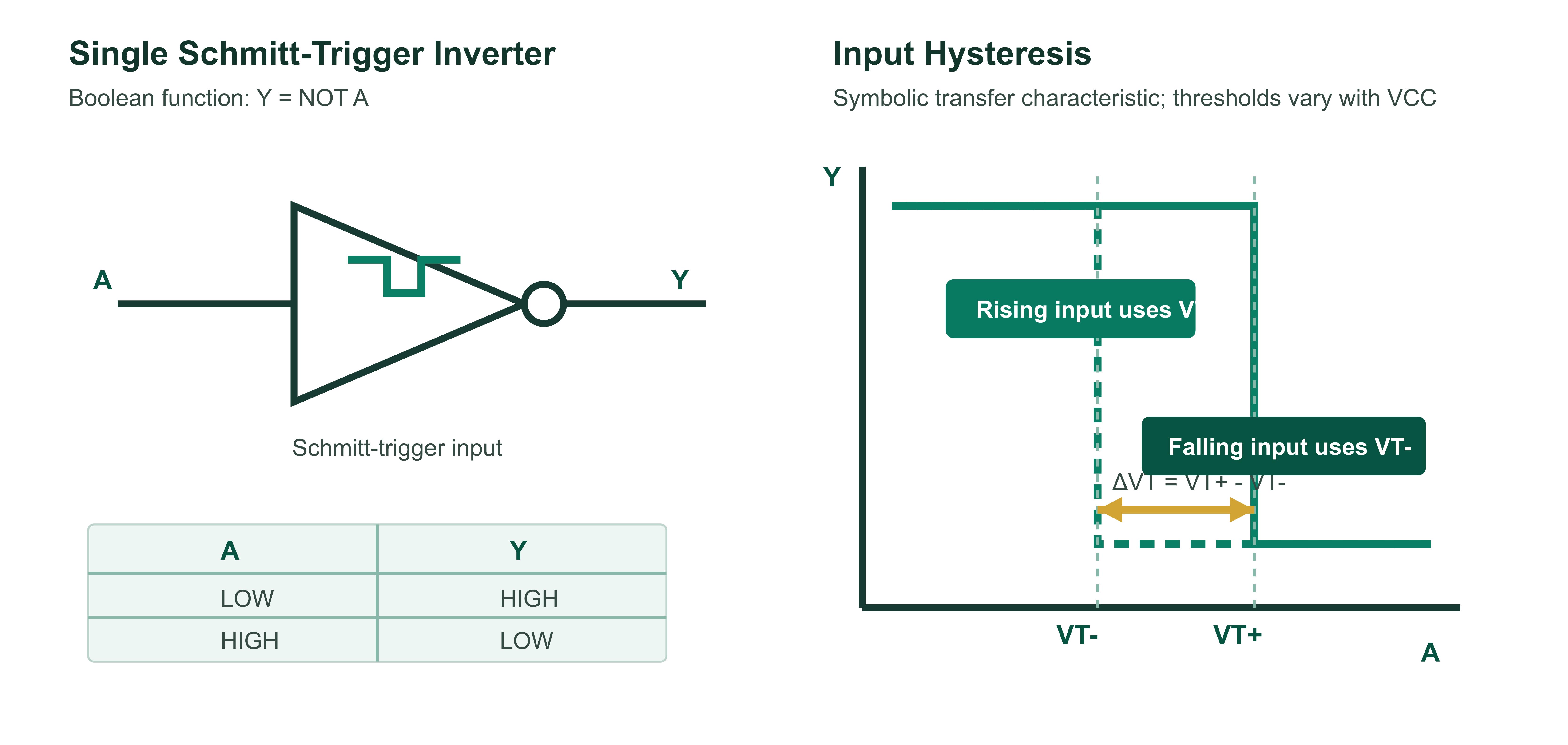
SN74AHCT1G14 contains one Schmitt-trigger inverter. In positive logic, the output is LOW when A is HIGH and HIGH when A is LOW. The input uses separate rising and falling thresholds, which creates a hysteresis window and improves immunity to slow edge transitions and noise near the switching point.
Signal role
One Schmitt-trigger input and one push-pull inverting output.
Voltage domain
Recommended VCC is 2.0 V to 5.5 V; input and output ranges are 0 V to 5.5 V.
Power-down behavior
Ioff is specified with VCC = 0 V to limit backflow through the powered-down output path.
Package
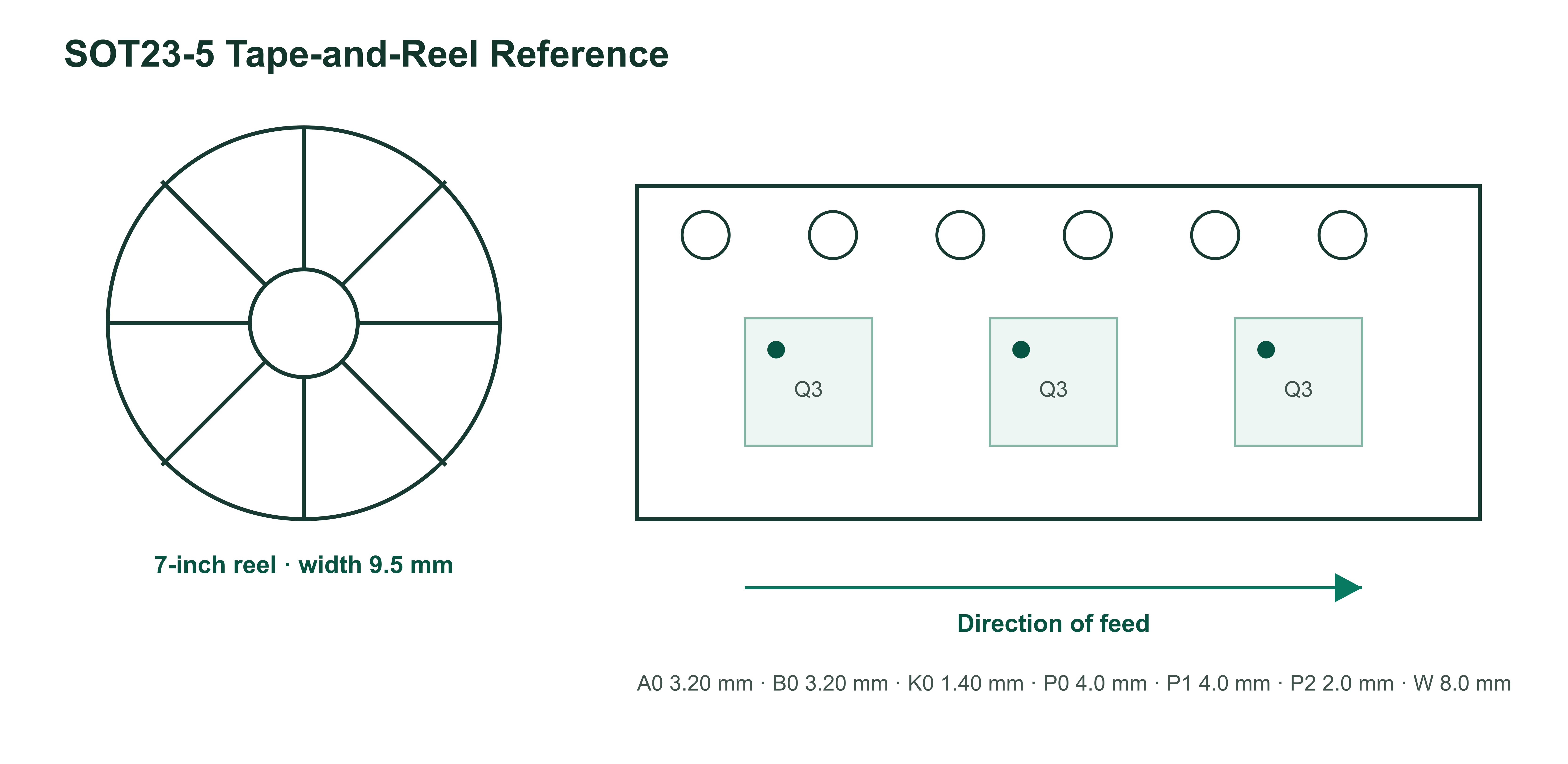
Green SOT23-5, ordering code SN74AHCT1G14DBVR, 3,000 units per tape-and-reel.
Selection boundary: A Schmitt-trigger input improves digital switching behavior, but the PDF does not specify analog comparator offset, input slew-rate measurement accuracy, oscillator frequency, fail-safe diagnostics or current-drive capability beyond the listed logic-output conditions.
Logic Function, Hysteresis and Pin Assignment
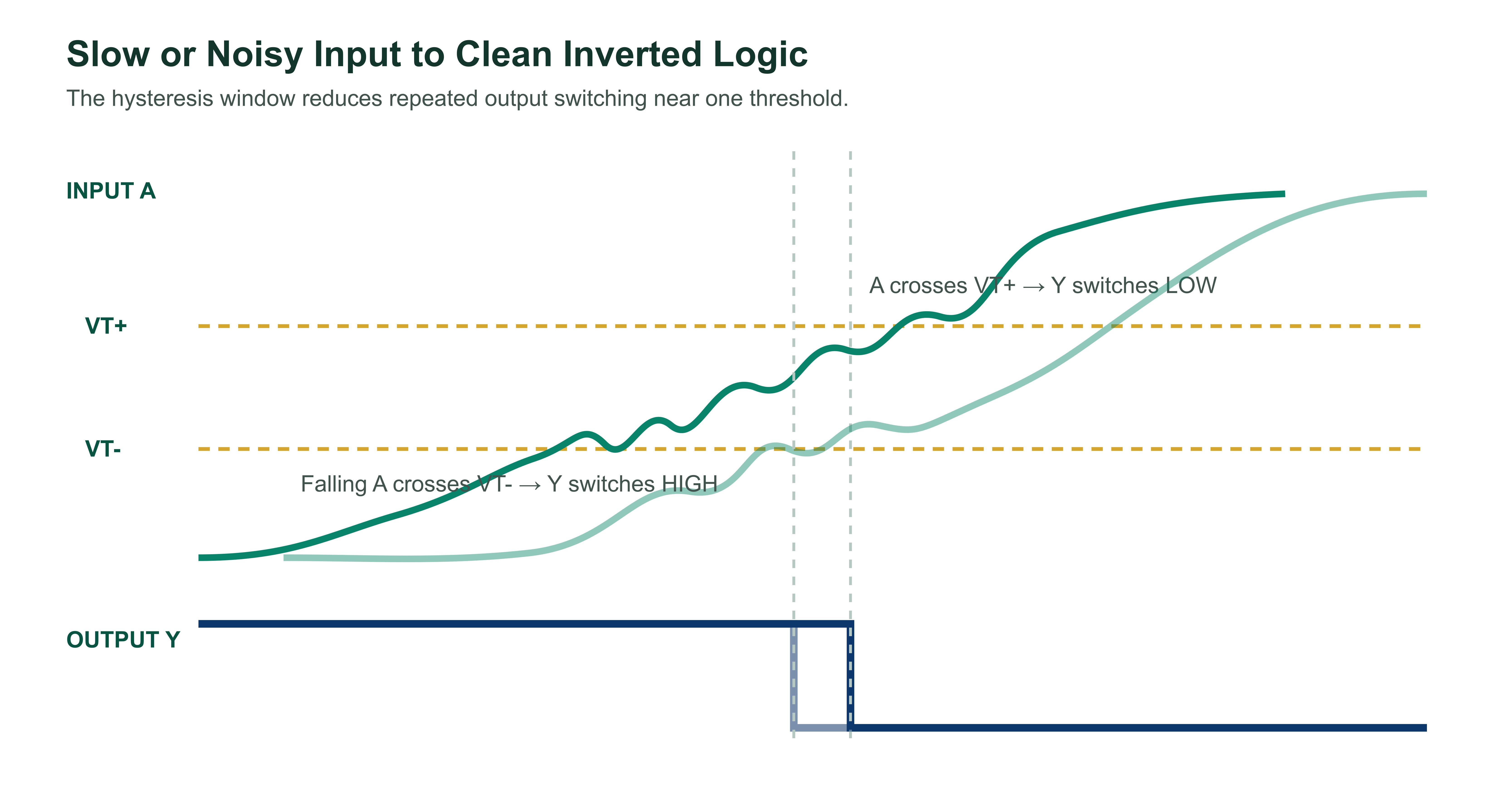
The Boolean function is Y = NOT A. A rising input is evaluated against VT+; a falling input is evaluated against VT-. Their difference, ΔVT, is the hysteresis window.
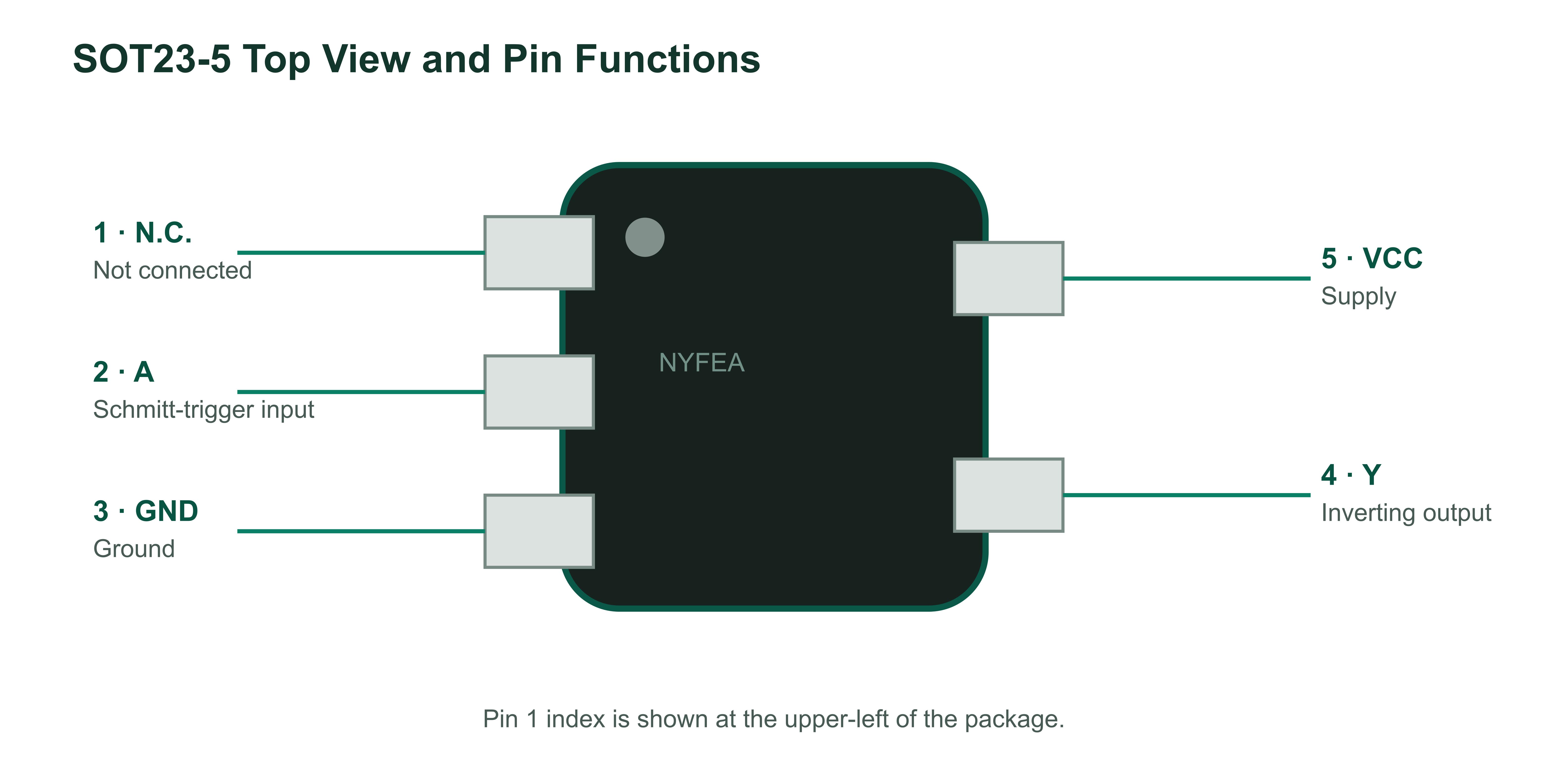
| Pin | Name | Type | Function | Engineering note |
|---|---|---|---|---|
| 1 | N.C. | - | Not connected | Do not use as a signal or return connection. |
| 2 | A | Input | Schmitt-trigger data input | Do not leave floating. |
| 3 | GND | Power | Ground | Use a short return to the local bypass capacitor. |
| 4 | Y | Output | Push-pull inverted output | Avoid bus contention and loads beyond the DC conditions. |
| 5 | VCC | Power | Supply | Place local decoupling near pins 5 and 3. |
Ordering Code and Package Selection
| Product | Ordering number | Temperature range | Package | Marking | MSL | Packing |
|---|---|---|---|---|---|---|
| SN74AHCT1G14 | SN74AHCT1G14DBVR | -40 °C to +125 °C | SOT23-5 | B14S | MSL 3 | Tape and reel, 3,000 units |
Additional lot, date, vendor, logo or environmental markings may appear. Confirm ordering code, top marking, reel orientation and current document revision at receiving inspection.
Recommended Operating Conditions and Absolute Limits
Recommended operating conditions define the functional design range. Absolute maximum ratings are stress limits and do not imply functional operation.
| Parameter | Symbol | Condition | Minimum | Maximum | Unit |
|---|---|---|---|---|---|
| Supply voltage | VCC | Operating | 2.0 | 5.5 | V |
| Input voltage | VI | Operating | 0 | 5.5 | V |
| Output voltage | VO | Operating | 0 | 5.5 | V |
| Ambient temperature | TA | Operating | -40 | +125 | °C |
Absolute maximum and handling limits
| Parameter | Condition | Minimum | Maximum | Unit |
|---|---|---|---|---|
| Supply voltage | VCC | -0.5 | 6.5 | V |
| Input voltage | VI | -0.5 | 6.5 | V |
| Output voltage, high-impedance or power-off | VO | -0.5 | 6.5 | V |
| Output voltage, HIGH or LOW state | VO | -0.5 | VCC + 0.5 | V |
| Input clamp current | VI < 0 V | - | -50 | mA |
| Output clamp current | VO < 0 V | - | -50 | mA |
| Continuous output current | IO | ±50 | mA | |
| Continuous VCC or GND current | - | ±100 | mA | |
| Junction temperature | TJ | - | 150 | °C |
| Storage temperature | Tstg | -65 | 150 | °C |
DC Characteristics and Schmitt-Trigger Thresholds
Unless otherwise noted, full-range limits apply from -40 °C to +125 °C. Typical values are characterized at +25 °C; they are not guaranteed limits.
| Parameter | VCC | Temperature | Minimum | Typical | Maximum | Unit |
|---|---|---|---|---|---|---|
| VT+ positive-going threshold | 2.0 V | Full | 0.7 | - | 1.2 | V |
| 3.3 V | 1.0 | - | 1.5 | |||
| 4.5 V to 5.5 V | 1.2 | - | 2.0 | |||
| VT- negative-going threshold | 2.0 V | Full | 0.3 | - | 0.6 | V |
| 3.3 V | 0.5 | - | 0.9 | |||
| 4.5 V to 5.5 V | 0.6 | - | 1.2 | |||
| ΔVT hysteresis | 2.0 V | Full | 0.3 | - | 0.8 | V |
| 3.3 V | 0.3 | - | 1.0 | |||
| 4.5 V to 5.5 V | 0.3 | - | 1.2 |
Output levels, leakage and supply current
| Parameter | Test condition | VCC | Temperature | Minimum / typical / maximum | Unit |
|---|---|---|---|---|---|
| VOH | IOH = -100 µA | 2.0 V to 5.5 V | Full | Minimum VCC - 0.1 V | V |
| VOH | IOH = -8 / -24 / -32 mA | 2.0 / 3.3 / 4.5 / 5.0 / 5.5 V | Full | Minimum 1.6 / 2.5 / 3.8 / 4.2 / 4.8 V | V |
| VOL | IOL = 100 µA | 2.0 V to 5.5 V | Full | Maximum 0.1 V | V |
| VOL | IOL = 8 / 24 / 32 mA | 2.0 / 3.3 / 4.5 / 5.0 / 5.5 V | Full | Maximum 0.45 / 0.55 / 0.55 / 0.50 / 0.45 V | V |
| II | A at 5.5 V or GND | 0 V to 5.5 V | +25 °C / Full | Typical ±0.1 µA / maximum ±10 µA | µA |
| Ioff | VI or VO = 5.5 V | 0 V | +25 °C / Full | Typical ±0.1 µA / maximum ±10 µA | µA |
| ICC | VI = 5.5 V or GND, IO = 0 | 2.0 V to 5.5 V | +25 °C / Full | Typical 0.1 µA / maximum 10 µA | µA |
| ICCT | Input at 3.4 V | 5.5 V | Full | Maximum 500 µA | µA |
AC Switching Characteristics and Measurement Conditions
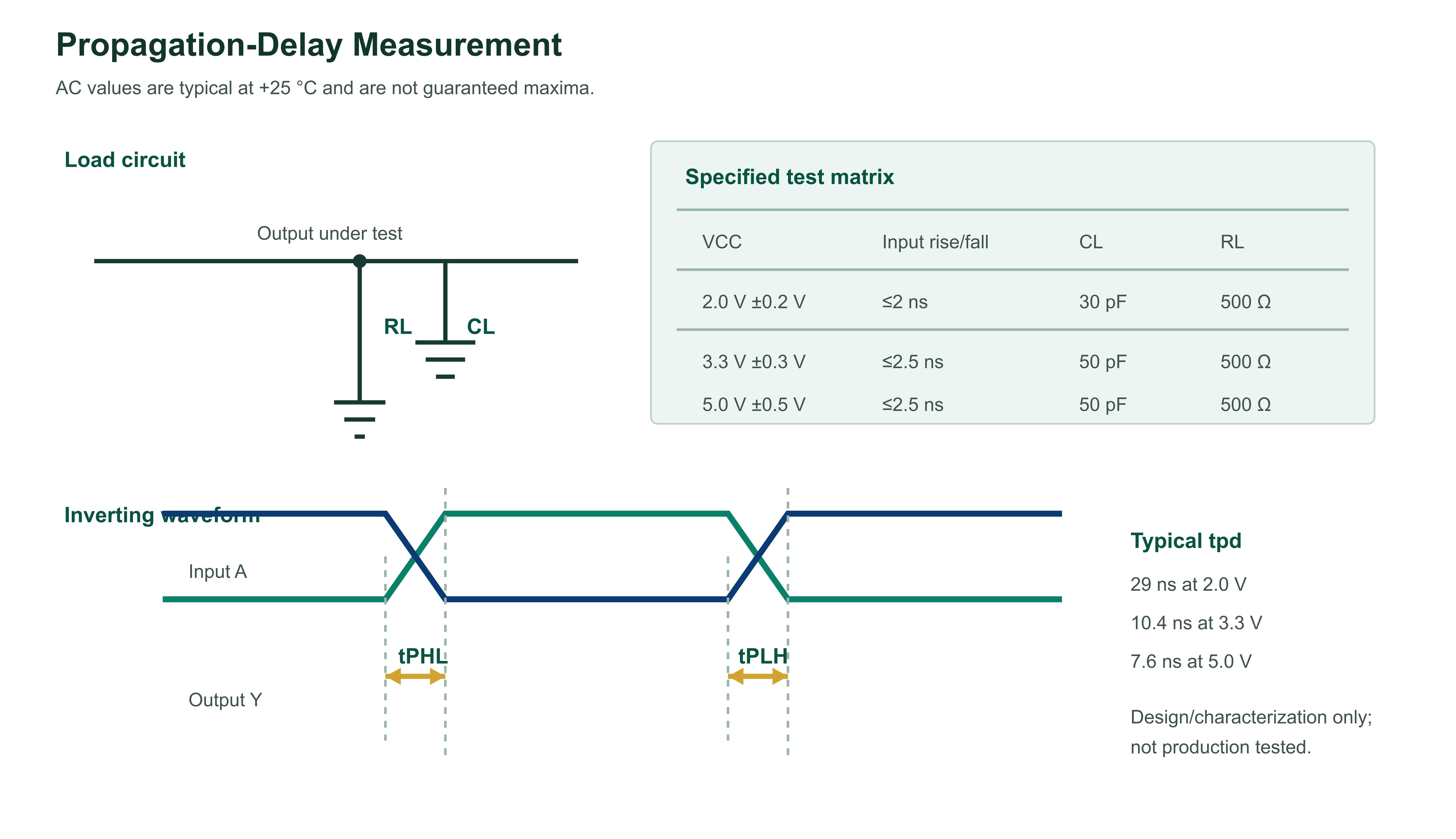
The PDF lists propagation-delay values at +25 °C as typical. It explicitly states that these parameters are ensured by design and/or characterization and are not tested in production.
| Parameter | VCC | Load | Temperature | Typical | Guaranteed maximum | Unit |
|---|---|---|---|---|---|---|
| Propagation delay, tpd | 2.0 V ±0.2 V | CL = 30 pF, RL = 500 Ω | +25 °C | 29 | Not specified | ns |
| Propagation delay, tpd | 3.3 V ±0.3 V | CL = 50 pF, RL = 500 Ω | +25 °C | 10.4 | Not specified | ns |
| Propagation delay, tpd | 5.0 V ±0.5 V | CL = 50 pF, RL = 500 Ω | +25 °C | 7.6 | Not specified | ns |
| Input capacitance, Ci | 5 V | VI = VCC or GND | +25 °C | 4.2 | Not specified | pF |
| Power-dissipation capacitance, Cpd | 5 V | f = 10 MHz | +25 °C | 16.6 | Not specified | pF |
Power Integrity, Input Handling and PCB Layout
Use a local bypass capacitor to supply transient output current and control rail disturbance. The complete product specification should govern the final decoupling strategy; 0.1 µF close to VCC and GND is the minimum practical local implementation for evaluation.
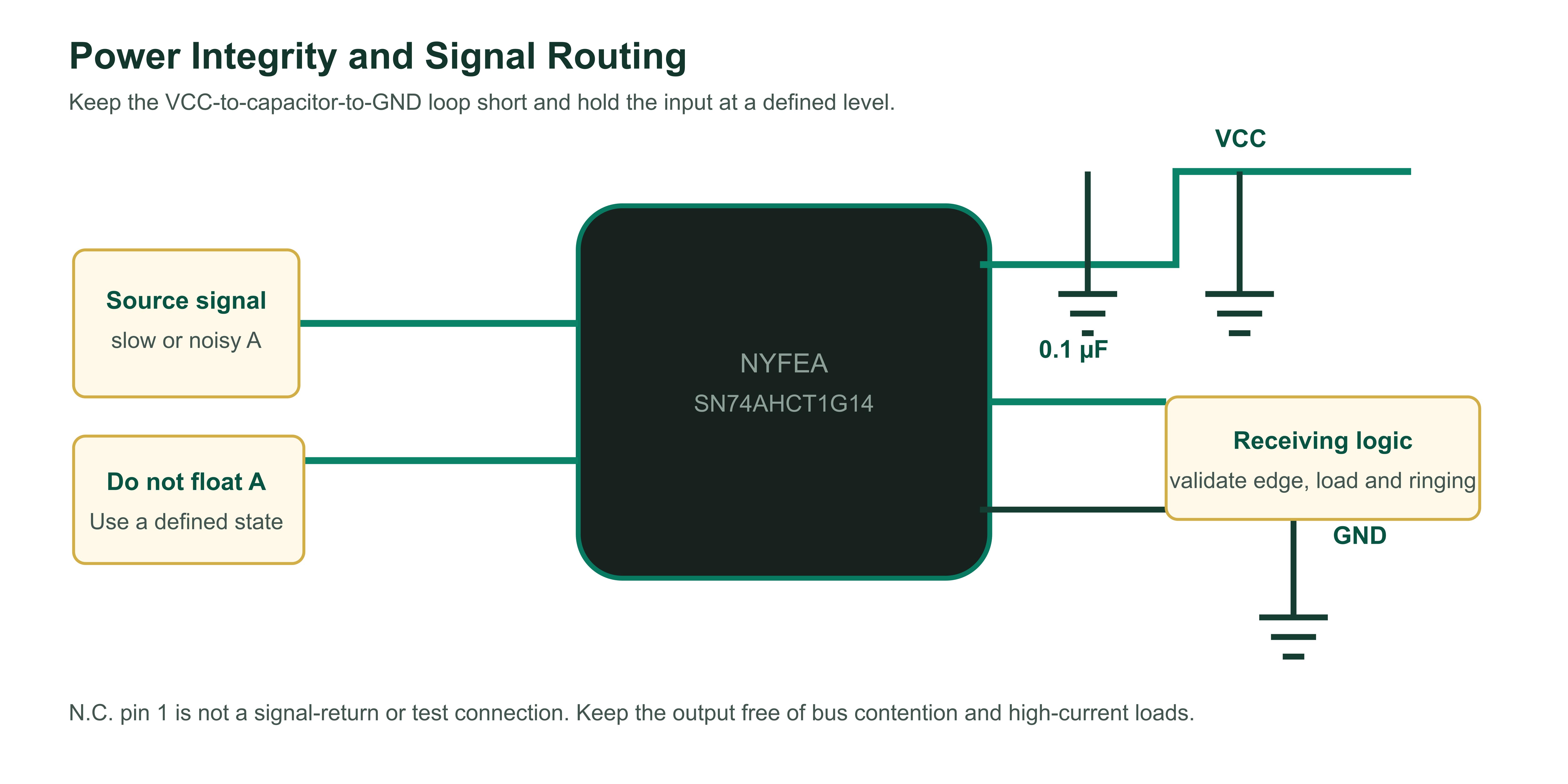
- Do not leave A floating: connect unused inputs to VCC or GND.
- Control the output load: ±32 mA is tied to the stated 5.0 V DC test conditions; it is not a general-purpose power-drive rating.
- Avoid contention: Y is a push-pull CMOS output, not open-drain and not tri-state.
- Check slow-edge behavior: hysteresis prevents threshold chatter, but ICCT and transition repetition still affect power.
- Validate partial power-down: Ioff characterizes the device path; total board back-powering through other components remains a system issue.
SOT23-5 Package, Land Pattern and Tape-and-Reel Data
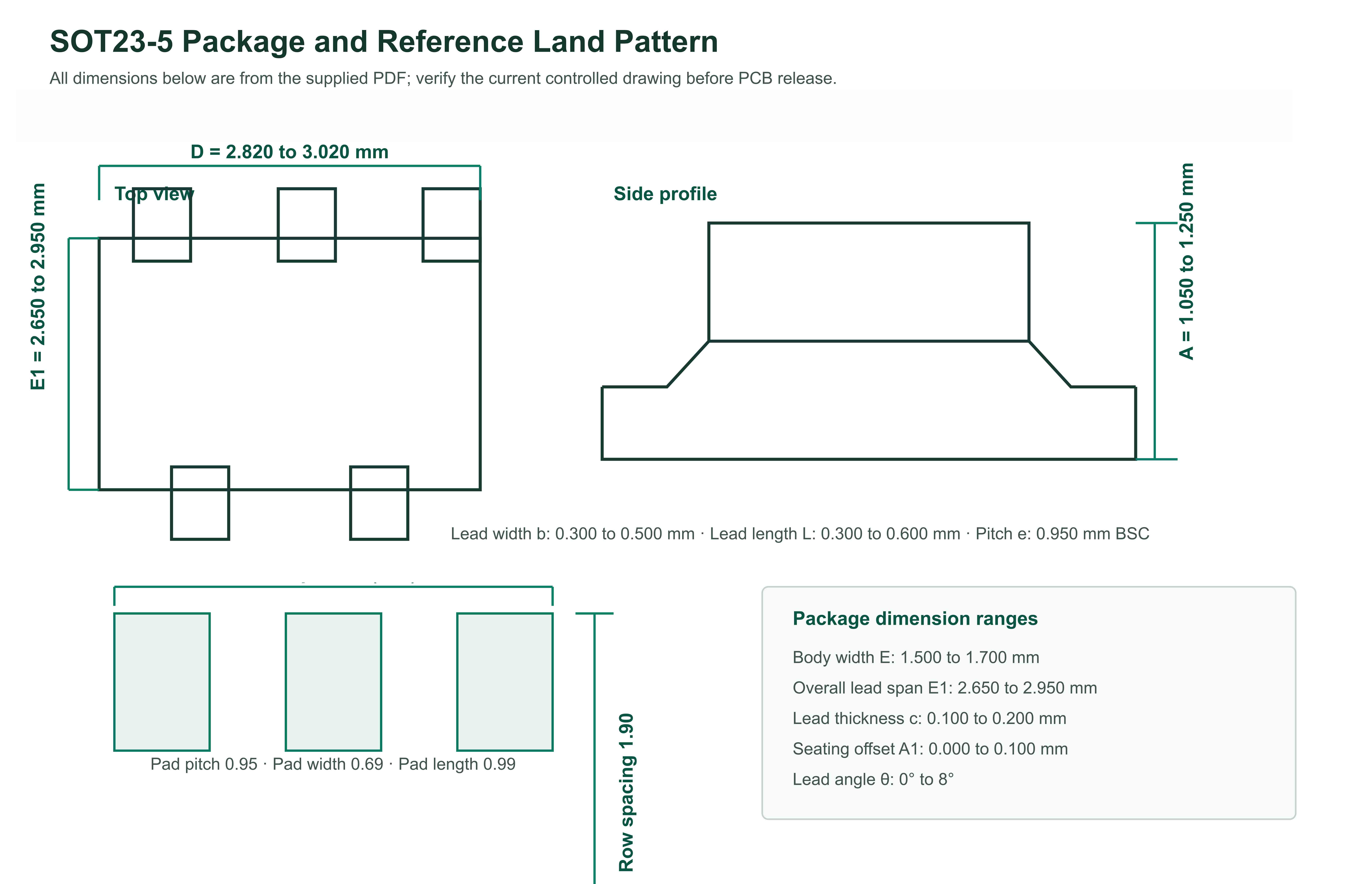
The single listed package is SOT23-5. Dimensions below reproduce the source drawing; PCB-library release must still use the complete controlled PDF and the assembler's land-pattern rules.
| Symbol | Minimum | Maximum | Unit | Meaning |
|---|---|---|---|---|
| A | 1.050 | 1.250 | mm | Overall height |
| A1 | 0.000 | 0.100 | mm | Seating offset |
| A2 | 1.050 | 1.150 | mm | Body height |
| b | 0.300 | 0.500 | mm | Lead width |
| c | 0.100 | 0.200 | mm | Lead thickness |
| D | 2.820 | 3.020 | mm | Body length |
| E | 1.500 | 1.700 | mm | Body width |
| E1 | 2.650 | 2.950 | mm | Overall lead span |
| e | 0.950 BSC | mm | Lead pitch | |
| e1 | 1.800 | 2.000 | mm | Outer lead pitch |
| L | 0.300 | 0.600 | mm | Lead length |
| θ | 0° | 8° | degree | Lead angle |
Application Guidance and Design Limitations
The supplied PDF lists AC receivers, Blu-ray players and home theaters, desktop or notebook PCs, digital video cameras, mobile phones, GPS devices and portable media players. These are application examples, not end-product qualification statements.
 AC ReceiverCondition a slowly changing or noise-affected control signal before digital logic. Validate input amplitude, threshold margin and transition rate.
 Blu-ray Players and Home TheatersUse for local reset, detect or control-signal cleanup. It does not process audio, video or high-current loads.
 Desktops or Notebook PCsApply to local logic qualification where TTL-compatible input behavior and one inverted output are appropriate.
 Digital Video Cameras (DVC)Condition a shutter, detect or camera-control signal after validating supply-domain compatibility, threshold margin and standby current.
 Personal Navigation Device (GPS)Use as a compact local inverter with hysteresis in a navigation control path; positioning accuracy, timing and system wake behavior remain external design responsibilities.
SN74AHCT1G14 Engineering FAQs
What logic function does SN74AHCT1G14 implement?
It is one Schmitt-trigger inverter. In positive logic, Y is LOW when A is HIGH and HIGH when A is LOW.
Why are VT+ and VT- different?
Separate rising and falling thresholds create hysteresis. The PDF specifies ΔVT ranges of 0.3 V to 0.8 V at 2.0 V, 0.3 V to 1.0 V at 3.3 V and 0.3 V to 1.2 V at 4.5 V to 5.5 V.
Can SN74AHCT1G14 accept a slow or noisy input?
The Schmitt-trigger input is intended to tolerate slow or noisy transitions better than a single-threshold input. Confirm that the signal crosses the guaranteed VT+ and VT- limits and include ICCT and transition activity in the power budget.
What is the recommended supply range?
VCC is specified from 2.0 V to 5.5 V under recommended operating conditions.
Is the 7.6 ns propagation delay a guaranteed maximum?
No. The PDF lists 7.6 ns as a typical value at +25 °C with VCC = 5.0 V ±0.5 V, CL = 50 pF and RL = 500 Ω. No maximum propagation-delay limit is listed.
What package and order code are listed?
The listed order code is SN74AHCT1G14DBVR in SOT23-5, top marking B14S, MSL 3, packed 3,000 units per reel.
What does Ioff provide?
Ioff is specified with VCC = 0 V and VI or VO = 5.5 V to reduce damaging current backflow through the powered-down device. Verify all other board-level back-power paths separately.
Can the output directly drive a high-current load?
Do not treat the ±32 mA statement as a general power rating. It is associated with stated 5.0 V DC output-level conditions; verify VOH/VOL, thermal dissipation, transient current and load behavior.
How should the device be decoupled?
Place a local bypass capacitor close to VCC and GND with a short return path. Add broader-frequency decoupling where required by the board power-distribution network.
Does the application list establish product certification?
No. It identifies possible use contexts only. Qualification, safety, EMC, reliability and production validation remain system responsibilities.
This page summarizes the SN74AHCT1G14 Rev A.1 product specification for component evaluation and engineering reference. It does not replace the complete controlled specification. Confirm the current revision, ordering code, marking, pin assignment, threshold limits, absolute maximum ratings, DC and AC conditions, package tolerances, PCB layout, assembly process and qualification requirements before production release.
