
01 · Device purpose
Product Overview and Selection Scope
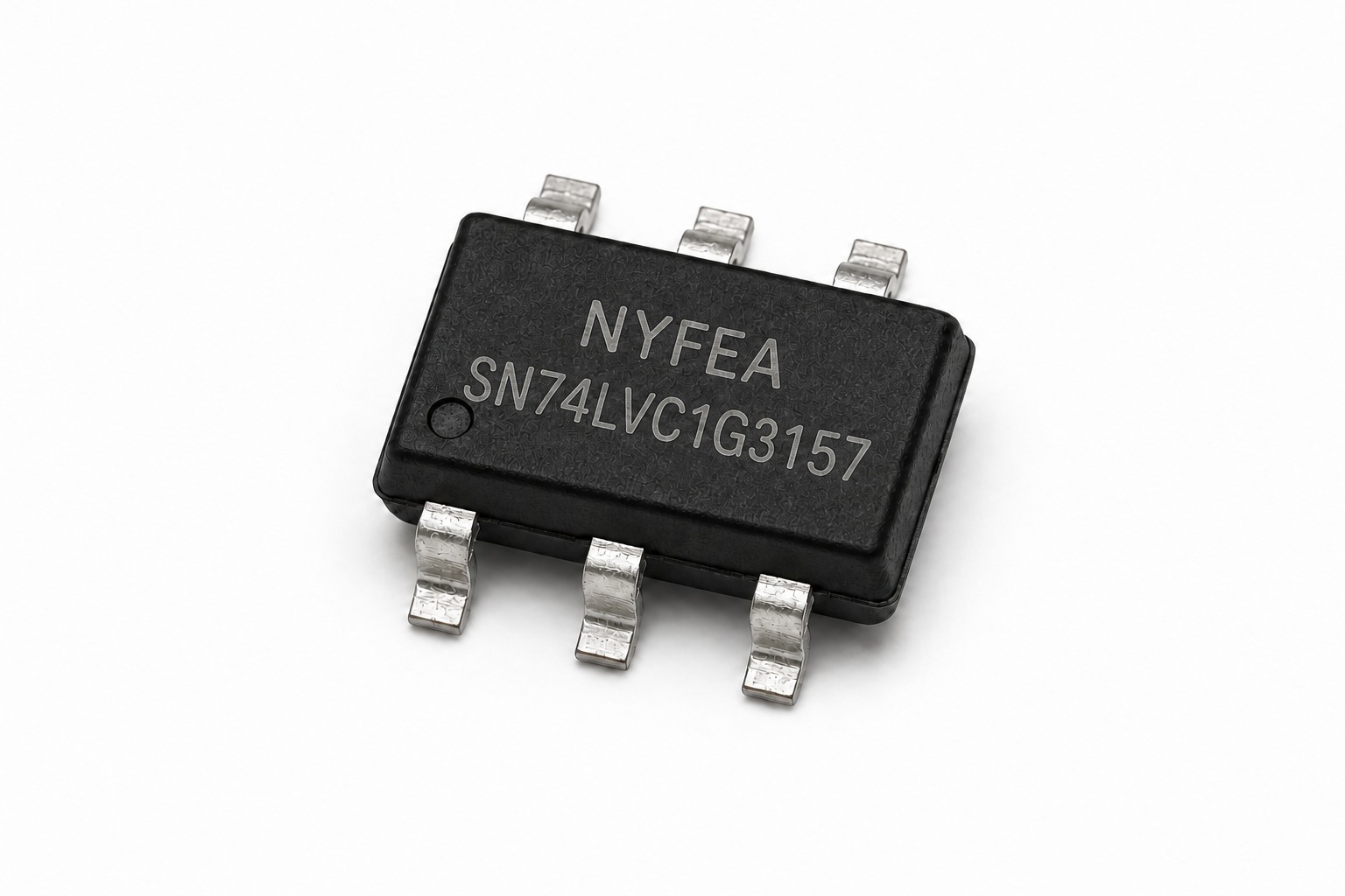
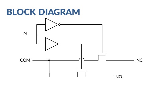
SN74LVC1G3157 is one bidirectional single-pole double-throw analog switch controlled by a digital IN pin.
- Low signal loss: 4.5 Ω typical on-resistance at V+ = 5 V.
- Wide signal bandwidth: 300 MHz typical -3 dB bandwidth with a 50 Ω load.
- Fast switching: 30 ns typical turn-on at 5 V and 25 ns typical turn-off at 5 V.
- Break-before-make: the active channel opens before the alternate channel closes.
- Rail-to-rail signal path: analog signals are specified from 0 V to V+.
- Analog or digital routing: NO, NC and COM are bidirectional signal terminals.
Selection boundary: This part is a passive analog signal switch with digital control. It is not a voltage regulator, gain stage, isolation barrier, high-current load switch or guaranteed over-voltage-tolerant signal path.
02 · Switching and pins
SPDT Routing, Control Logic and Pin Assignment
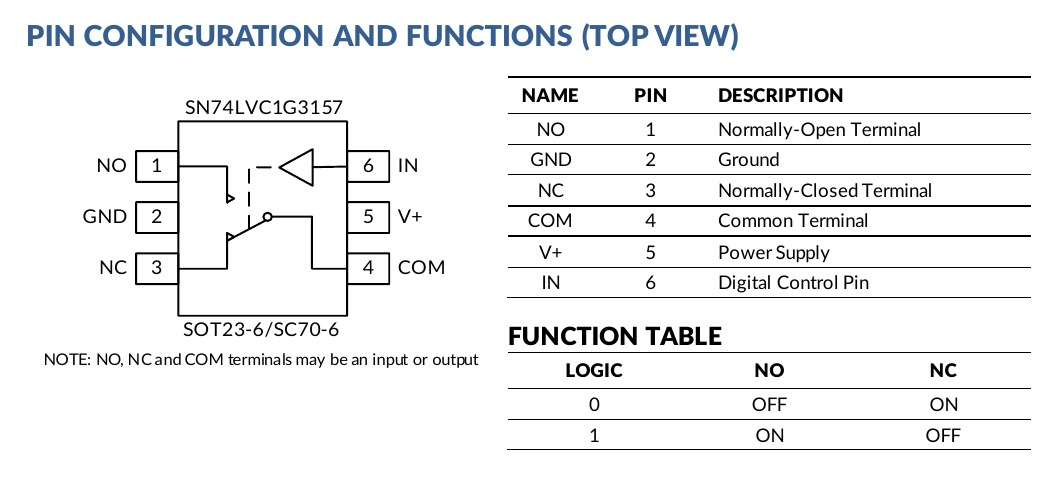
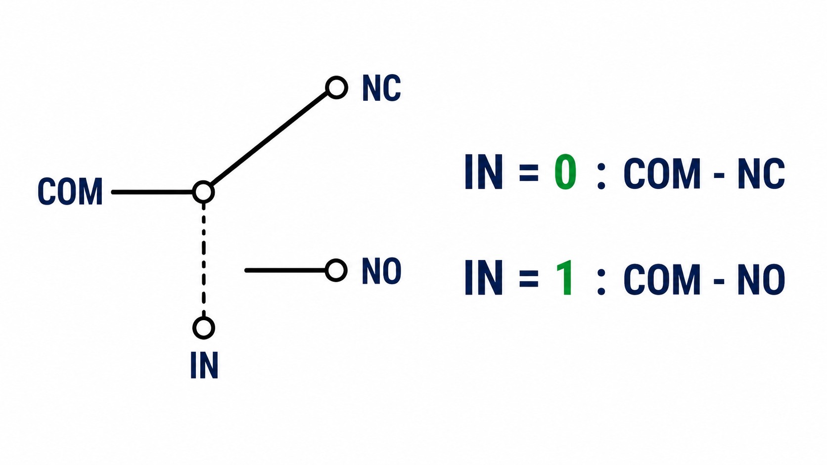
IN LOW selects the normally closed path from COM to NC. IN HIGH selects the normally open path from COM to NO. The signal terminals are bidirectional.
| Pin | Name | Type | Function | Engineering note |
|---|---|---|---|---|
| 1 | NO | Analog I/O | Normally open signal terminal | Connected to COM when IN is HIGH. |
| 2 | GND | Power | Ground | Use a short local return path. |
| 3 | NC | Analog I/O | Normally closed signal terminal | Connected to COM when IN is LOW. |
| 4 | COM | Analog I/O | Common signal terminal | Bidirectional; selected to NC or NO. |
| 5 | V+ | Power | Positive supply | Place local bypass capacitance close to pins 5 and 2. |
| 6 | IN | Digital input | Channel-select control | LOW selects NC; HIGH selects NO. |
03 · Orderable options
Ordering Codes and Package Selection
| Ordering number | Temperature range | Package listed in PDF | Top marking | MSL | Packing |
|---|---|---|---|---|---|
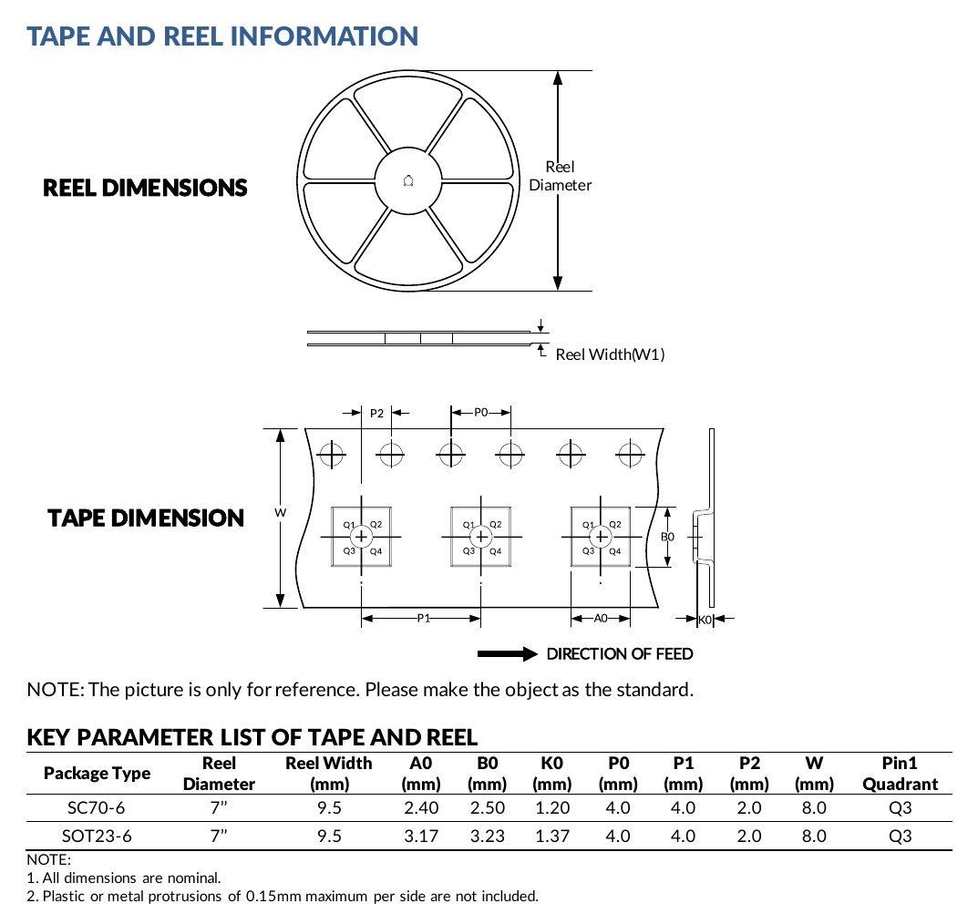
| SN74LVC1G3157DBVR | -40 °C to +125 °C | SC70-6 / SOT363 equivalent | CC5F | MSL 3 | Tape and reel, 3,000 units |
| SN74LVC1G3157DCKR | -40 °C to +125 °C | SOT23-6 | 3157 | MSL 3 | Tape and reel, 3,000 units |
The package mapping above follows the supplied PDF. Confirm the complete orderable code, package and top marking against controlled purchasing documentation before release.
04 · Design envelope
Operating Conditions, Signal Range and Absolute Limits
| Parameter | Condition | Minimum | Maximum | Unit |
|---|---|---|---|---|
| Supply voltage, V+ | Operating | 1.8 | 5.5 | V |
| Analog signal voltage | NO, NC or COM | 0 | V+ | V |
| Digital input HIGH, VINH | V+ = 5 V / 3.3 V | 1.5 / 1.3 | - | V |
| Digital input LOW, VINL | V+ = 5 V / 3.3 V | - | 0.6 / 0.5 | V |
| Ambient temperature, TA | Operating | -40 | 125 | °C |
Absolute maximum and handling limits
| Parameter | Minimum | Maximum | Unit |
|---|---|---|---|
| Supply voltage, V+ | -0.3 | 6.0 | V |
| Digital input voltage | -0.3 | 6.0 | V |
| Analog / digital terminal voltage | -0.3 | V+ + 0.3 | V |
| Continuous current at NO, NC or COM | -300 | +300 | mA |
| Peak current at NO, NC or COM | -500 | +500 | mA |
| Junction temperature | - | 150 | °C |
| Storage temperature | -65 | 150 | °C |
05 · Signal-path performance
On-Resistance, Leakage and Control Thresholds
| Parameter | Condition | V+ | Typical | Full-range maximum |
|---|---|---|---|---|
| On-resistance, RON | Signal = V+/2, ICOM = -10 mA | 5 V | 4.5 Ω | 8.5 Ω |
| On-resistance, RON | Signal = V+/2, ICOM = -10 mA | 3.3 V | 7 Ω | 10.5 Ω |
| Channel RON match, ΔRON | Signal = V+/2, ICOM = -10 mA | 5 V / 3.3 V | 0.15 Ω | 0.4 Ω |
| RON flatness | 0 V to V+/2, ICOM = -10 mA | 5 V | 2 Ω | 3.3 Ω |
| RON flatness | 0 V to V+/2, ICOM = -10 mA | 3.3 V | 3 Ω | 4.3 Ω |
| OFF leakage | NO or NC off | 1.8 V to 5.5 V | - | 1 µA |
| ON leakage | Selected channel on | 1.8 V to 5.5 V | - | 1 µA |
| Control input leakage | IN at supply or ground | 1.8 V to 5.5 V | - | 1 µA |
| Supply current | IN at ground or V+ | 5.5 V | - | 1 µA |
06 · Dynamic performance
Switching Time, Break-Before-Make and Bandwidth
| Parameter | 5 V typical | 3.3 V typical | Condition / unit |
|---|---|---|---|
| Turn-on time, tON | 30 | 40 | ns at +25 °C, RL = 300 Ω, CL = 35 pF |
| Turn-off time, tOFF | 25 | 30 | ns at +25 °C, RL = 300 Ω, CL = 35 pF |
| Break-before-make delay, tBBM | 5 | 8 | ns at +25 °C, RL = 300 Ω, CL = 35 pF |
| Off isolation | -52 dB at 10 MHz; -71 dB at 1 MHz | Typical, RL = 50 Ω | |
| -3 dB bandwidth | 300 MHz | Typical, switch ON, RL = 50 Ω | |
| OFF capacitance | 5 pF | Typical at +25 °C | |
| ON capacitance | 15 pF | Typical at +25 °C | |
07 · Implementation
Signal Integrity, Control and PCB Guidance
- Stay within the rails: keep the analog signal from 0 V to V+ in normal operation.
- Use break-before-make wisely: the device reduces momentary channel overlap, but system timing and charge injection still require validation.
- Control IN firmly: tie unused digital inputs to V+ or GND and verify the listed thresholds at the actual supply.
- Minimize parasitics: use short routes and a continuous return reference for wide-band signals.
- Budget insertion loss: include worst-case RON, receiver impedance, source impedance and connector resistance.
- Bypass locally: place a 0.1 µF capacitor close to V+ and GND.
System check: Validate bandwidth, distortion, off isolation, crosstalk, charge injection, switching transients, signal amplitude, source impedance and PCB parasitics in the finished design.
08 · Mechanical
SC70-6 and SOT23-6 Packages, Land Patterns and Packing
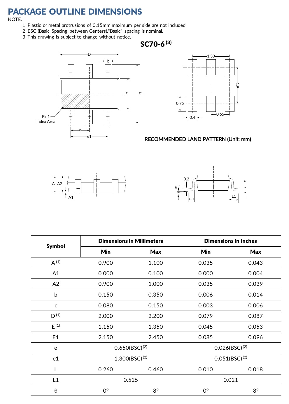
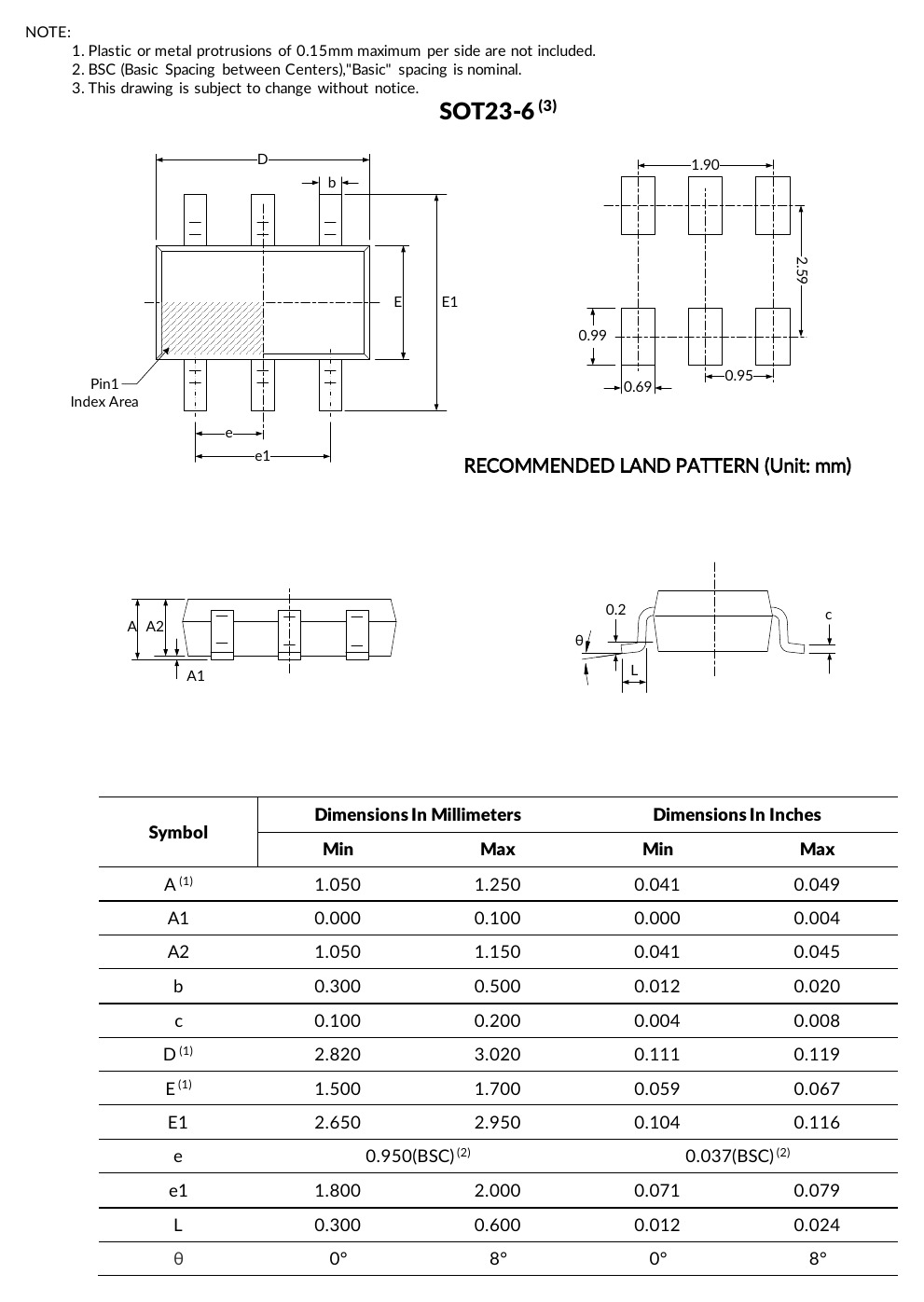
The packages share the same logical pin assignment but have different body dimensions, lead pitch, marking and thermal impedance. Do not share one PCB footprint between them.
| Dimension | SC70-6 | SOT23-6 | Unit |
|---|---|---|---|
| Overall height A | 0.900 to 1.100 | 1.050 to 1.250 | mm |
| Body length D | 2.000 to 2.200 | 2.820 to 3.020 | mm |
| Body width E | 1.150 to 1.350 | 1.500 to 1.700 | mm |
| Overall lead span E1 | 2.150 to 2.450 | 2.650 to 2.950 | mm |
| Lead pitch e | 0.650 BSC | 0.950 BSC | mm |
| Outer lead pitch e1 | 1.300 BSC | 1.800 to 2.000 | mm |
| Lead width b | 0.150 to 0.350 | 0.300 to 0.500 | mm |
| Lead length L | 0.260 to 0.460 | 0.300 to 0.600 | mm |
09 · Use contexts
Application Guidance and Design Limitations
The supplied specification lists the following application areas. These are use contexts, not end-product approvals or safety certifications.
 Wearable DevicesRoute compact sensor or user-interface signals after full system validation.
 Battery-Operated EquipmentSelect analog or digital paths with low static supply current.
 Signal Gating and ModemsSupport chopping, modulation, demodulation and conversion-path multiplexing.
 Portable ComputingSwitch board-level signal paths in space-constrained computing hardware.
 Cell PhonesRoute low-voltage signals after bandwidth and distortion checks.
10 · Engineering answers
SN74LVC1G3157 Engineering FAQs
What function does SN74LVC1G3157 implement?
It is an SPDT analog switch. IN LOW connects COM to NC, and IN HIGH connects COM to NO.
Can NO, NC and COM be used in either signal direction?
Yes. The PDF states that NO, NC and COM may be inputs or outputs.
What signal range is recommended?
Analog signals should remain between 0 V and V+ during normal operation.
What is the typical on-resistance?
RON is typically 4.5 Ω at V+ = 5 V and 7 Ω at V+ = 3.3 V under the specified midpoint and -10 mA test condition.
What does break-before-make mean?
The currently selected channel opens before the alternate channel closes, reducing momentary conduction between NO and NC during switching.
What supply range is recommended?
V+ is specified from 1.8 V to 5.5 V.
Which packages are listed?
The supplied PDF lists SN74LVC1G3157DBVR as SC70-6 with CC5F marking and SN74LVC1G3157DCKR as SOT23-6 with 3157 marking. Both are MSL 3 and tape-and-reel packed in quantities of 3,000.
Can the digital control input be left open?
No. Every unused digital input must be held at V+ or GND.
This page summarizes the supplied SN74LVC1G3157 Rev A.1 product specification for component evaluation. Confirm the current controlled specification, ordering code, marking, pin assignment, electrical limits, package tolerances and qualification requirements before production release.
