
FRTC1337S Low-Power I²C Real-Time Clock with Dual Time-of-Day Alarms
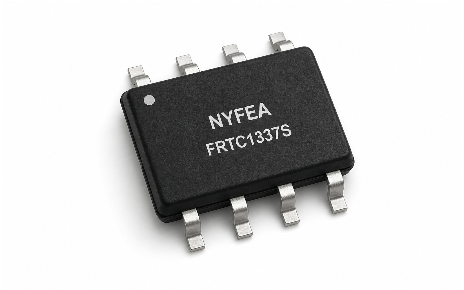
NYFEA FRTC1337S is a 1.8 V to 5.5 V I²C real-time clock with an external 32.768 kHz crystal, two programmable time-of-day alarms, oscillator-stop detection and a programmable square-wave output.
Product scope: FRTC1337S is a calendar RTC IC. It requires an external 32.768 kHz crystal, I²C pull-up resistors and system firmware for initialization, coherent time reads, alarm servicing and oscillator-stop validation. It does not include a backup-supply pin.
Use the current controlled PDF for register definitions, timing, test conditions, package dimensions and production release decisions.
Product Overview and Scope
NYFEA FRTC1337S is a 1.8 V to 5.5 V I²C real-time clock with an external 32.768 kHz crystal, two programmable time-of-day alarms, oscillator-stop detection and a programmable square-wave output.
Selection boundary: Similar I²C functionality or pin count does not establish drop-in compatibility with another RTC. Compare address, registers, oscillator and power architecture before committing a PCB or firmware migration.
Key Features
Calendar
Seconds, minutes, hours, day, date, month and year in BCD; 12/24-hour operation and leap-year correction.
Alarms
Two time-of-day alarms with maskable repeat rates and open-drain interrupt routing.
Square wave
Selectable 1 Hz, 4.096 kHz, 8.192 kHz or 32.768 kHz output.
Clock supervision
Oscillator-stop flag supports startup and time-validity checks.
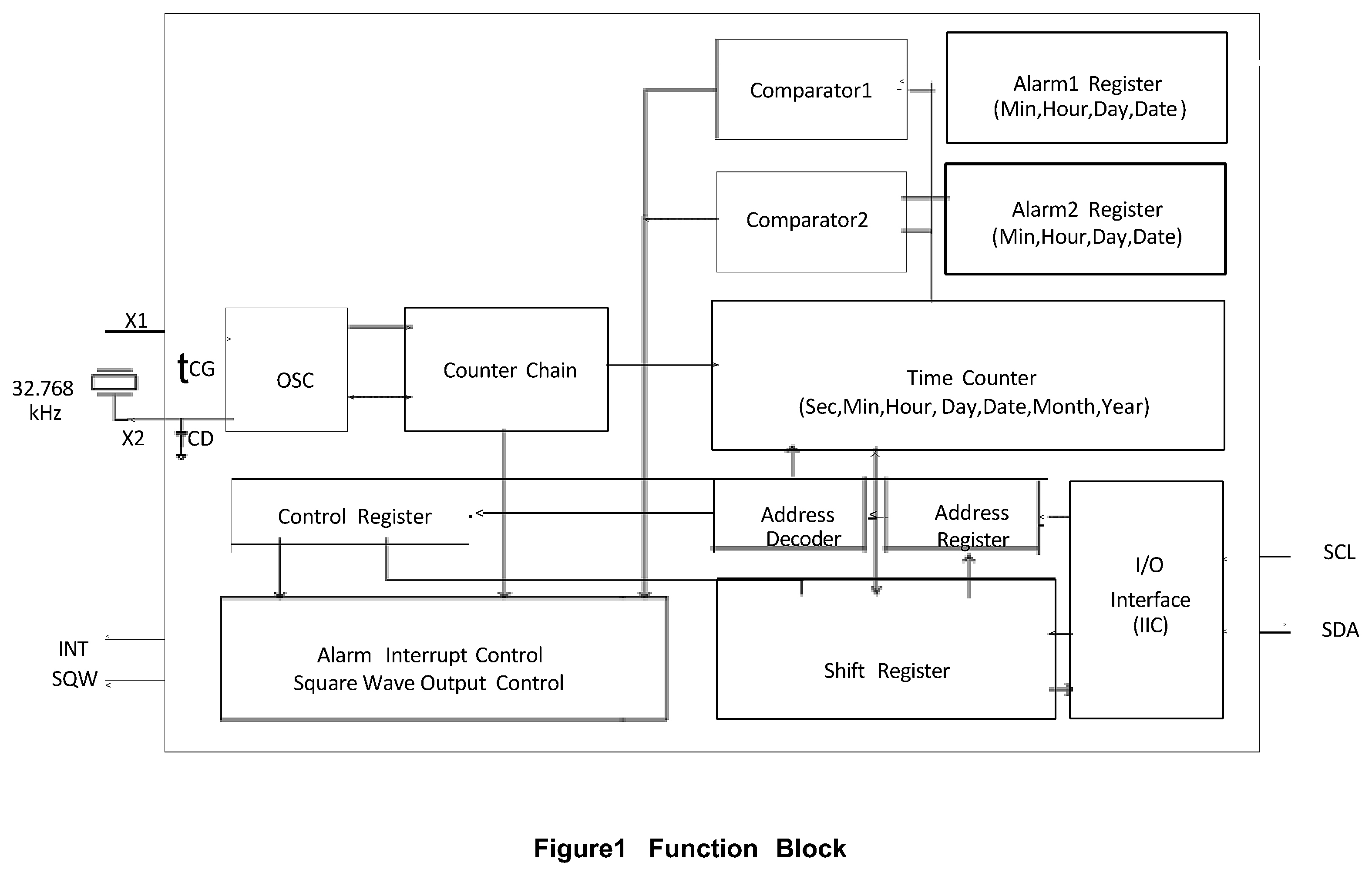
Function Block
The functional block diagram shows how the oscillator, divider and calendar logic, control/status registers, host interface and output or interrupt functions are connected inside FRTC1337S.
Timekeeping and Calendar Operation
The calendar is encoded in BCD unless the controlled PDF states otherwise. Firmware should use a coherent multi-byte read, validate field ranges and apply the device-specific century and leap-year rules.
| Calendar | Seconds, minutes, hours, day, date, month and year in BCD; 12/24-hour operation and leap-year correction. |
|---|---|
| Alarms | Two time-of-day alarms with maskable repeat rates and open-drain interrupt routing. |
| Square wave | Selectable 1 Hz, 4.096 kHz, 8.192 kHz or 32.768 kHz output. |
| Clock supervision | Oscillator-stop flag supports startup and time-validity checks. |
I²C Interface, Outputs and Interrupts
| Host interface | I²C, up to 400 kHz |
|---|---|
| 7-bit slave address | 1101000b (0x68) |
| Output and interrupt scope | Alarms, square-wave output and clock supervision |
| Pull-up requirement | SDA and the open-drain interrupt/output pins require external pull-up resistors selected for the logic rail, bus capacitance and required rise time. |
| Firmware responsibility | Initialize the control registers, read and clear status flags, and use a coherent multi-byte access procedure around calendar rollovers. |
Read Mode
To read from a selected register, the controller first writes the register address, issues a repeated START, and then addresses FRTC1337S for reading. The device returns data beginning at the selected register. For a multi-byte read, the controller acknowledges each byte that is followed by another byte; it terminates the final byte with NACK and then issues STOP.
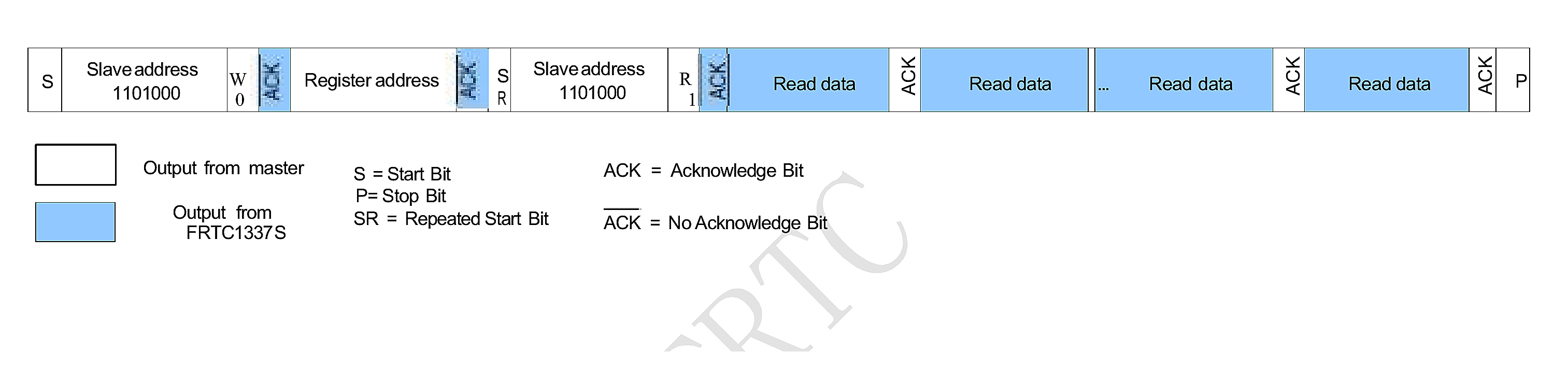
- Use the write phase only to select the starting register; no register data is written during this phase.
- Use a repeated START before the read address phase.
- End the last received byte with NACK before STOP; otherwise the device interprets an ACK as a request for another byte.
Write Mode
For a write transfer, the controller sends START, the 7-bit slave address with the write bit, and the target register address. One or more data bytes then follow. FRTC1337S acknowledges the accepted address and each accepted data byte; STOP completes the transaction.
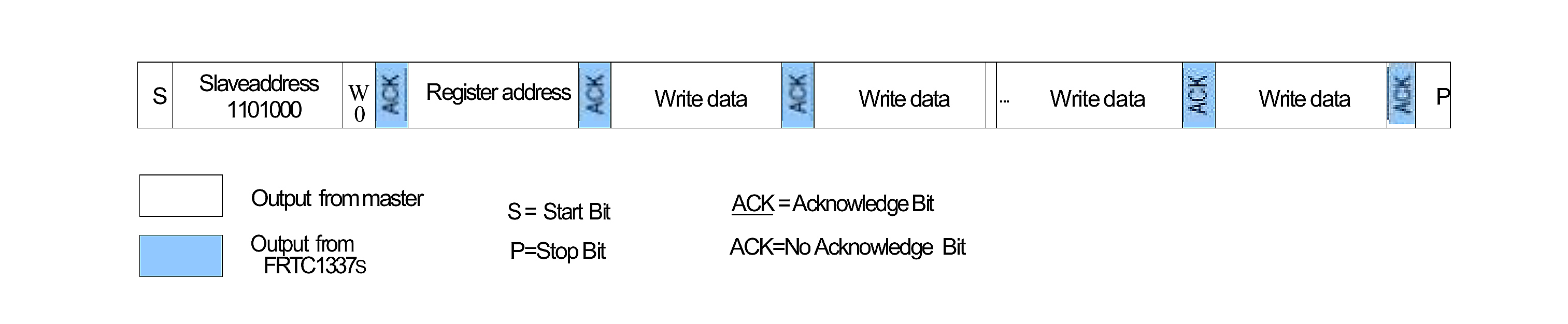
- Write only defined register values and preserve reserved bits as required by the register description.
- After writing time or control registers, read back the programmed values and confirm the relevant status flags.
Power, Backup and Time-Validity Strategy
| Primary supply | 1.8 V to 5.5 V |
|---|---|
| Timekeeping / backup | 1.7 V to 5.5 V oscillator range |
| Backup architecture | No dedicated backup-supply pin |
| Retained user memory | No general-purpose NVRAM stated |
| Current condition | Active supply current: 150 µA max under the stated 400 kHz test condition; standby: 0.5 µA typ., 0.8 µA max under the specified condition |
Current values are meaningful only with the adjacent voltage, interface, output and temperature conditions. Estimate system backup life from the worst-case current, source capacity after derating, leakage paths, pull-ups and switchover behavior.
Electrical Conditions and Accuracy
| Operating supply | 1.8 V to 5.5 V |
|---|---|
| Timekeeping / backup condition | 1.7 V to 5.5 V oscillator range |
| I²C interface | I²C, up to 400 kHz |
| Operating temperature | -40 °C to +85 °C |
| Current condition | Active supply current: 150 µA max under the stated 400 kHz test condition; standby: 0.5 µA typ., 0.8 µA max under the specified condition |
| Accuracy / stability | Set by the selected crystal, loading, PCB parasitics, temperature and calibration of the finished assembly |
| Package | SOP-8, 1.27 mm pitch |
PDF audit note: The operating and electrical tables consistently support -40 °C to +85 °C and 1.8 V to 5.5 V operation.
Typical Application Circuit
This product-level circuit shows the complete FRTC1337S connection concept from the controlled PDF: host I²C lines, external pull-ups, crystal network, supply decoupling, interrupt/output pull-ups and ground connection. It is not a complete end-product schematic; power sequencing, energy-source selection, EMC protection and production test remain system responsibilities.
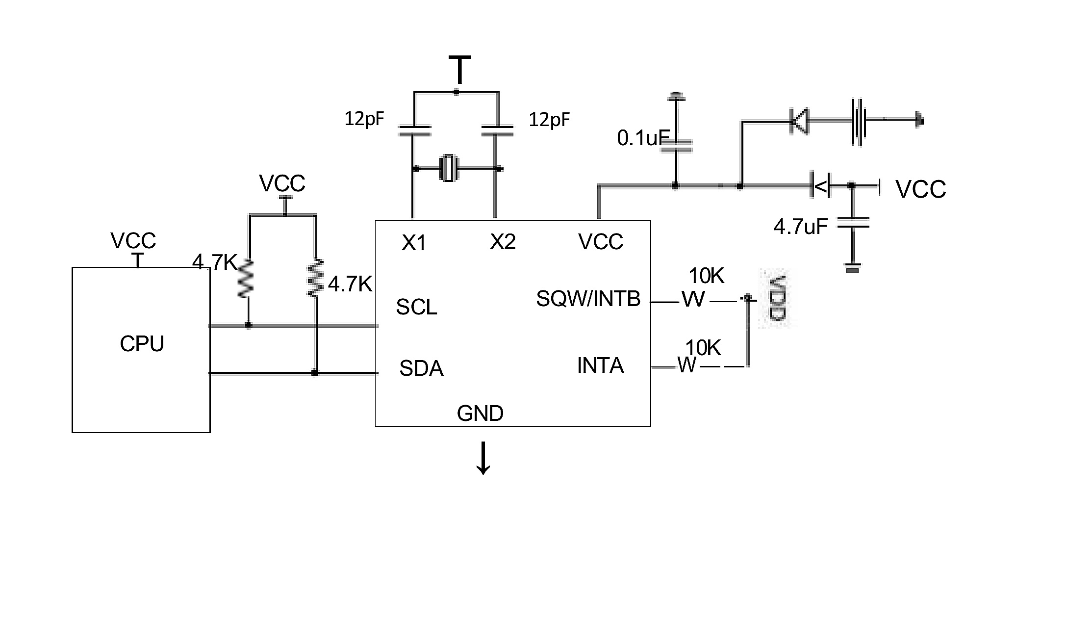
- Provide pull-up resistors for SDA, SCL, INTA and SQW/INTB according to the selected logic rail and bus loading.
- Place the supply bypass capacitor close to the VCC and GND pins and keep the high-current return paths away from the oscillator area.
- Use the oscillator-stop status as a time-validity indicator and initialize the calendar and control registers before accepting timestamps.
Recommended Layout for Crystal
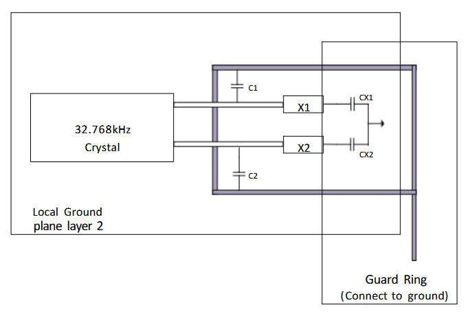
Place the 32.768 kHz crystal immediately beside X1 and X2. Keep the oscillator loop short, surround it with a grounded guard ring, and provide the local ground plane arrangement shown in the specification. The crystal, oscillator traces and X1/X2 pins should be isolated from RF-generating signals and fast switching nodes.
Package Information
Available package: SOP-8 with 1.27 mm lead pitch. The drawing below includes the package outline, terminal identification, dimension table and recommended land pattern. All dimensions are in millimetres unless otherwise stated.
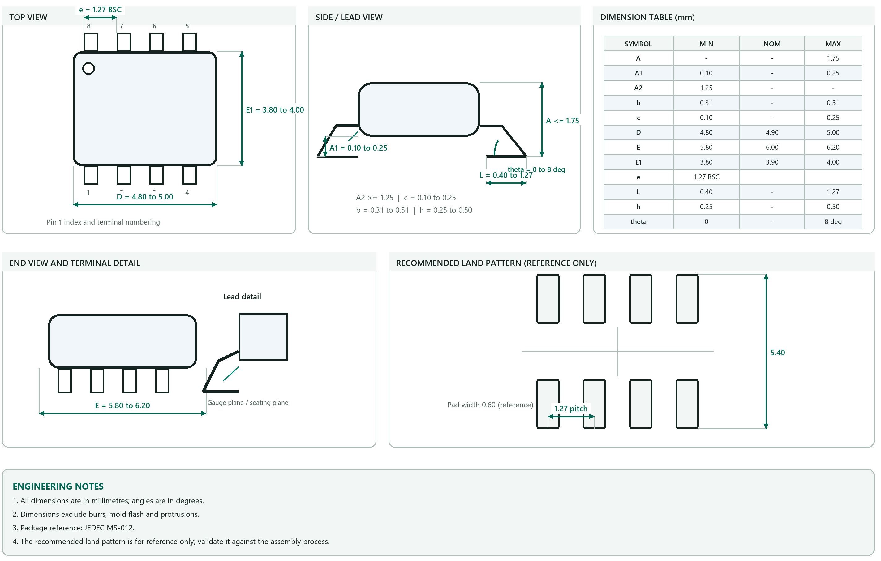
Package dimensions exclude burrs, mould flash and protrusions as stated in the PDF. Do not use the rendered product appearance image for pin numbering or dimensional inspection.
Application Guidance and Design Limitations
The controlled product specification explicitly lists portable instruments, electronic metering and telecom equipment. The notes below explain how the RTC functions relate to those listed applications without extending the product claim to unlisted markets.
 Portable Instruments
Use the calendar, dual alarms and square-wave output for local timekeeping and scheduled host events. The final instrument must provide the external 32.768 kHz crystal, pull-up resistors, initialization and oscillator-stop validation.
Portable Instruments
Use the calendar, dual alarms and square-wave output for local timekeeping and scheduled host events. The final instrument must provide the external 32.768 kHz crystal, pull-up resistors, initialization and oscillator-stop validation.
 Electronic Metering
Use RTC time for interval records, service events or display functions. Measurement data storage, billing integrity, legal-time requirements and recovery from invalid time remain responsibilities of the completed meter.
Electronic Metering
Use RTC time for interval records, service events or display functions. Measurement data storage, billing integrity, legal-time requirements and recovery from invalid time remain responsibilities of the completed meter.
 Telecom Equipment
Use retained calendar time for local event logs and maintenance schedules. FRTC1337S has no dedicated backup-supply pin, so any hold-up or source-selection function must be implemented and validated externally.
Telecom Equipment
Use retained calendar time for local event logs and maintenance schedules. FRTC1337S has no dedicated backup-supply pin, so any hold-up or source-selection function must be implemented and validated externally.
FRTC1337S Engineering FAQs
What is the FRTC1337S?
FRTC1337S is a NYFEA I²C real-time clock device. FRTC1337S is a calendar RTC IC. It requires an external 32.768 kHz crystal, I²C pull-up resistors and system firmware for initialization, coherent time reads, alarm servicing and oscillator-stop validation. It does not include a backup-supply pin.
What supply range does FRTC1337S use?
The controlled PDF specifies 1.8 V to 5.5 V. The timekeeping or backup condition is listed separately as 1.7 V to 5.5 V oscillator range.
Does FRTC1337S include a crystal?
External 32.768 kHz crystal; specified ESR up to 70 kΩ; internal capacitance listed as 12 pF.
What is the FRTC1337S operating temperature range?
The supported operating range used on this page is -40 °C to +85 °C.
Can FRTC1337S replace another RTC without redesign?
Do not infer a drop-in replacement from a similar function, interface or package. Verify pinout, I²C address, register map, power-fail behavior, oscillator network, interrupt handling, package dimensions and firmware in the final system.
How should time validity be checked after power-up?
Initialize the device as required, inspect the available oscillator-stop or voltage-status flags, perform a coherent calendar read and reject timestamps until the system has established a valid time source.
This page summarizes the FRTC1337S product specification for product evaluation and engineering reference. It does not replace the complete controlled specification. Confirm the current revision, register definitions, pin configuration, interface timing, absolute maximum ratings, oscillator and backup requirements, package dimensions, PCB layout, assembly process and qualification requirements before production release.
Download FRTC1337S Product SpecificationContact NYFEA for Product Support