
FRTC1338S I²C Real-Time Clock with 56-Byte Battery-Backed NV RAM
NYFEA FRTC1338S is a 3.3 V I²C real-time clock with an external 32.768 kHz crystal, 56 bytes of battery-backed NV RAM, automatic power-fail switching and a programmable square-wave output.
Product scope: FRTC1338S combines BCD timekeeping and 56 bytes of NV SRAM. The recommended VCC table specifies 2.97 V to 3.63 V; the page therefore does not generalize the feature-page reference to 1.8 V operation as a guaranteed VCC range.
Use the current controlled PDF for register definitions, timing, test conditions, package dimensions and production release decisions.
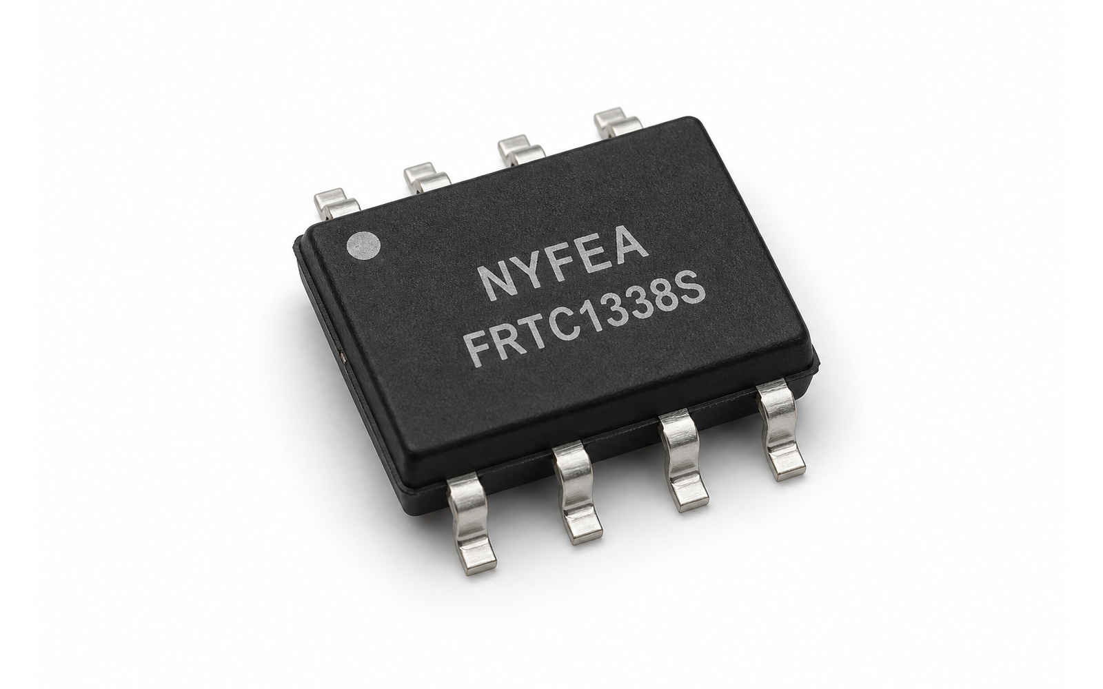
Product Overview and Scope
NYFEA FRTC1338S is a 3.3 V I²C real-time clock with an external 32.768 kHz crystal, 56 bytes of battery-backed NV RAM, automatic power-fail switching and a programmable square-wave output.
Selection boundary: Similar I²C functionality or pin count does not establish drop-in compatibility with another RTC. Compare address, registers, oscillator and power architecture before committing a PCB or firmware migration.
Key Features
Calendar
Seconds through year, 12/24-hour operation and leap-year compensation valid through 2100 as stated.
NV SRAM
56 bytes retained from the backup supply.
Square wave
Selectable 1 Hz, 4 kHz, 8 kHz or 32 kHz output.
Power supervision
Automatic power-fail detection and backup-source switching.
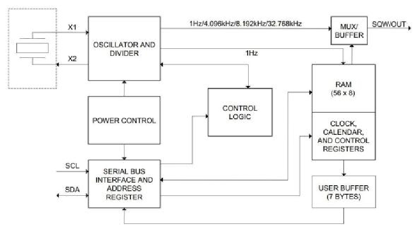
Function Block
The functional block diagram shows how the oscillator, divider and calendar logic, control/status registers, host interface and output or interrupt functions are connected inside FRTC1338S.
Timekeeping and Calendar Operation
The calendar is encoded in BCD unless the controlled PDF states otherwise. Firmware should use a coherent multi-byte read, validate field ranges and apply the device-specific century and leap-year rules.
| Calendar | Seconds through year, 12/24-hour operation and leap-year compensation valid through 2100 as stated. |
|---|---|
| NV SRAM | 56 bytes retained from the backup supply. |
| Square wave | Selectable 1 Hz, 4 kHz, 8 kHz or 32 kHz output. |
| Power supervision | Automatic power-fail detection and backup-source switching. |
I²C Interface, Outputs and Interrupts
| Host interface | I²C, up to 400 kHz |
|---|---|
| Output and interrupt scope | NV SRAM; Square wave; Power supervision |
| Pull-up requirement | SDA and open-drain interrupt/output pins require external pull-up resistors sized for the selected bus voltage and capacitance. |
| Firmware responsibility | Initialize control registers, read status flags, clear interrupt sources and prevent calendar rollover errors during multi-byte access. |
Power, Backup and Time-Validity Strategy
| Primary supply | VCC 2.97 V to 3.63 V |
|---|---|
| Timekeeping / backup | VBAT 1.3 V to 3.7 V in the recommended-condition table |
| Backup architecture | Automatic power-fail detection and switchover to VBAT; reads and writes are inhibited below the power-fail threshold |
| Retained user memory | 56 bytes battery-backed NV SRAM |
| Current condition | Active supply current: 120 µA typ., 200 µA max at the stated maximum SCL condition; standby: 85 µA typ., 125 µA max with the I²C bus inactive |
Current values are meaningful only with the adjacent voltage, interface, output and temperature conditions. Estimate system backup life from the worst-case current, source capacity after derating, leakage paths, pull-ups and switchover behavior.
Electrical Conditions and Accuracy
| Operating supply | VCC 2.97 V to 3.63 V |
|---|---|
| Timekeeping / backup condition | VBAT 1.3 V to 3.7 V in the recommended-condition table |
| I²C interface | I²C, up to 400 kHz |
| Operating temperature | -40 °C to +85 °C |
| Current condition | Active supply current: 120 µA typ., 200 µA max at the stated maximum SCL condition; standby: 85 µA typ., 125 µA max with the I²C bus inactive |
| Accuracy / stability | Determined by crystal tolerance, load match, PCB parasitics and temperature |
| Package | SOP-8 |
PDF audit note: The PDF feature list mentions several nominal logic rails, but the recommended VCC range is 2.97 V to 3.63 V; the latter is used as the engineering selection range.
Typical Application Circuit
The circuit is a product-level connection reference, not a complete end-product schematic. The host, power sequencing, energy source, EMC protection and production test strategy remain system responsibilities.
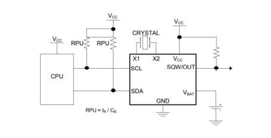
- Use the recommended crystal and keep X1/X2 traces short, guarded and isolated from clocks and RF sources.
- Connect VBAT only within its specified range; ground VBAT when backup operation is not required, as directed by the specification.
- After power-up, explicitly clear the clock-halt bit and initialize registers because the initial state is not guaranteed.
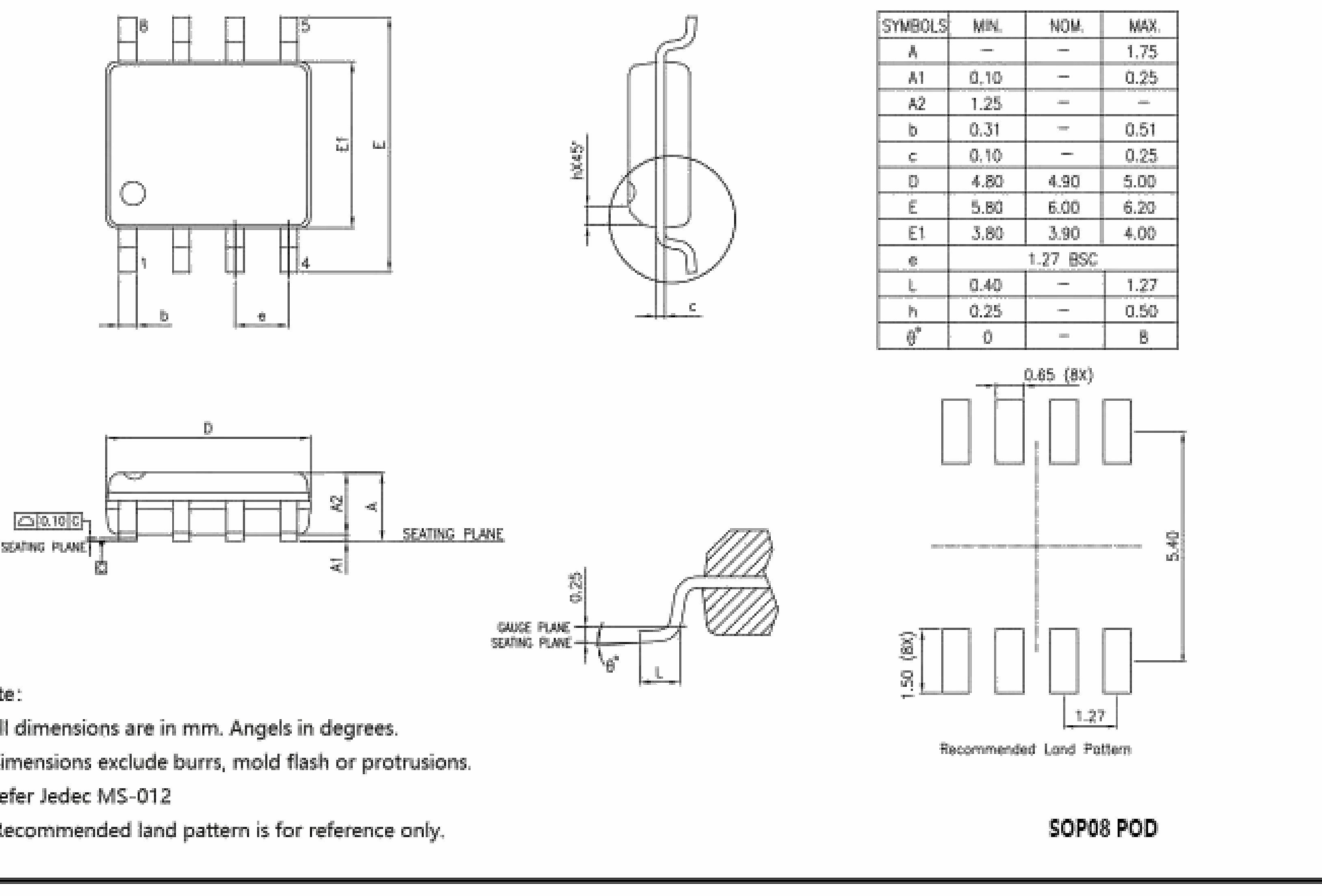
Package Information
Available package: SOP-8. Mechanical dimensions and terminal numbering are package-specific and must not be inferred from the product appearance image.
Application Guidance and Design Limitations
The controlled product specification explicitly lists the six application groups below. The listed examples identify evaluation contexts; they do not constitute finished-product certification or a guarantee of system-level performance.
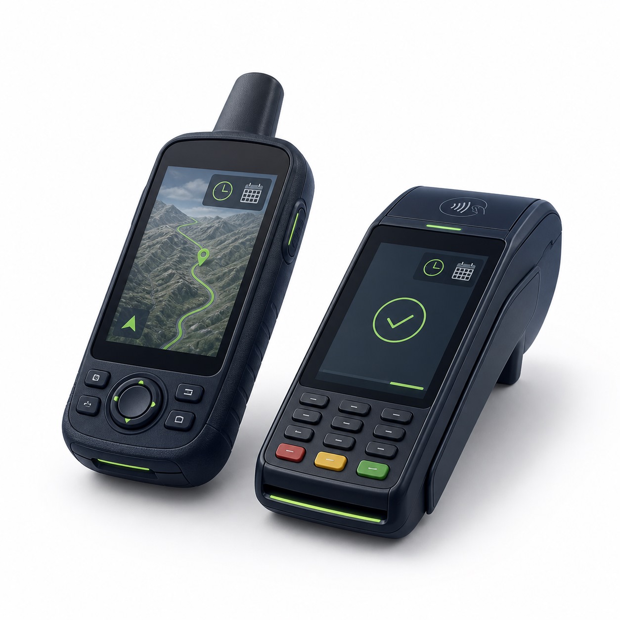 Handheld GPS and POS Terminals
Use the calendar, battery switchover and 56-byte battery-backed NV RAM for local time and small retained state. Validate backup-source endurance, write timing and time validity after power loss.
Handheld GPS and POS Terminals
Use the calendar, battery switchover and 56-byte battery-backed NV RAM for local time and small retained state. Validate backup-source endurance, write timing and time validity after power loss.
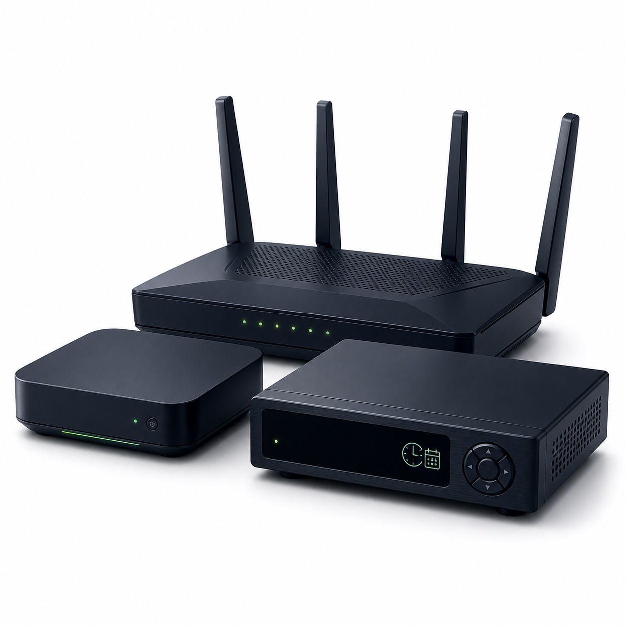 Consumer and Network Appliances
The PDF lists set-top boxes, digital recording equipment and network appliances. Scheduled operation and local logs must be designed around the specified VCC range, crystal network and power-fail behavior.
Consumer and Network Appliances
The PDF lists set-top boxes, digital recording equipment and network appliances. Scheduled operation and local logs must be designed around the specified VCC range, crystal network and power-fail behavior.
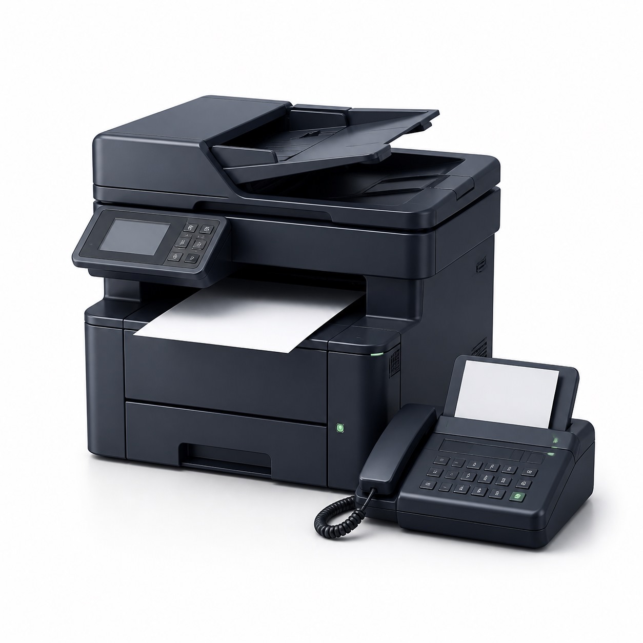 Office Equipment
The PDF lists fax machines, printers and copiers. Confirm oscillator placement, I²C pull-ups, backup operation and immunity to motor, switching-supply and cable noise in the assembled product.
Office Equipment
The PDF lists fax machines, printers and copiers. Confirm oscillator placement, I²C pull-ups, backup operation and immunity to motor, switching-supply and cable noise in the assembled product.
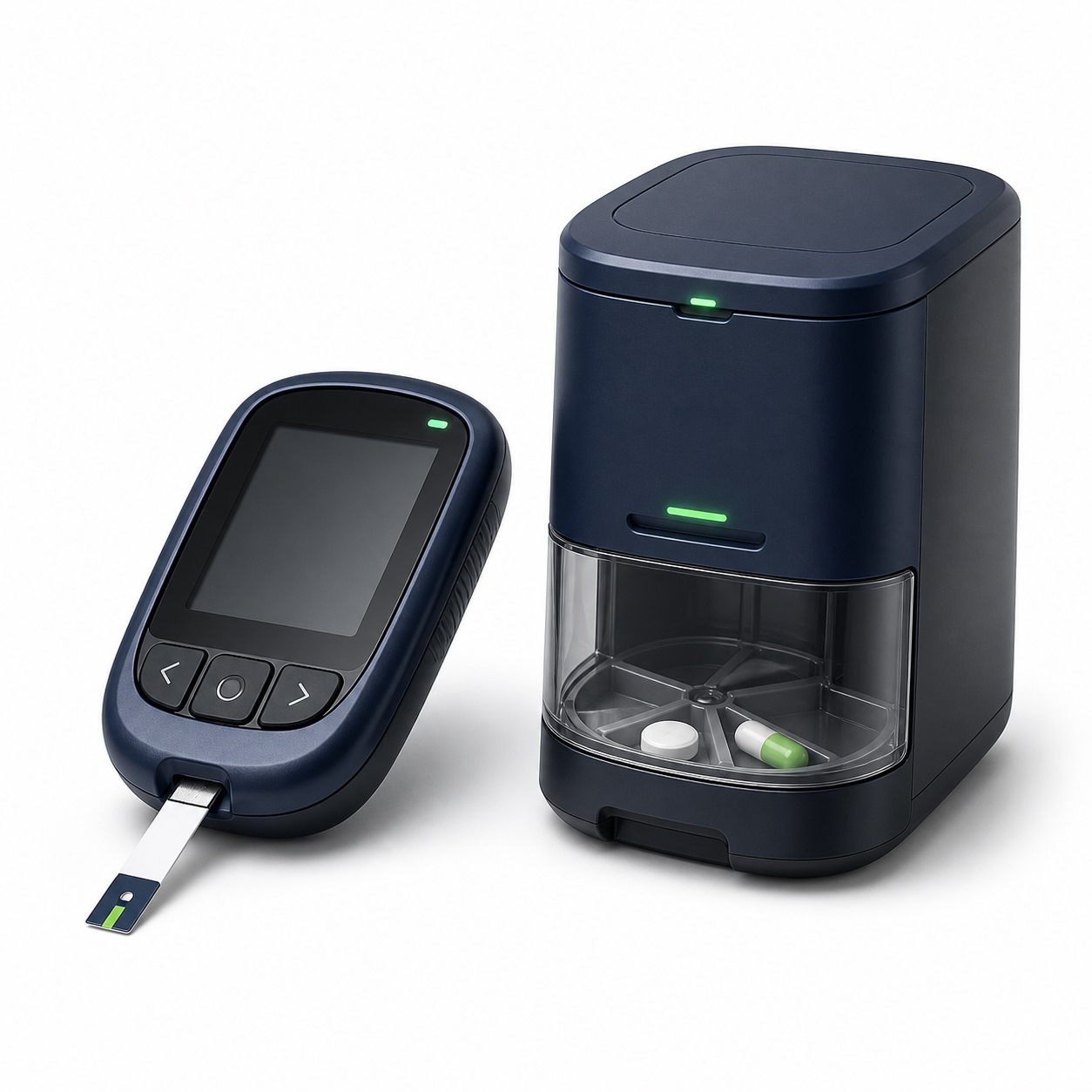 Medical Equipment
The PDF lists glucometers and medicine dispensers. Product safety, regulatory approval, risk control, timestamp integrity and failure response require independent validation; the RTC listing does not establish medical compliance.
Medical Equipment
The PDF lists glucometers and medicine dispensers. Product safety, regulatory approval, risk control, timestamp integrity and failure response require independent validation; the RTC listing does not establish medical compliance.
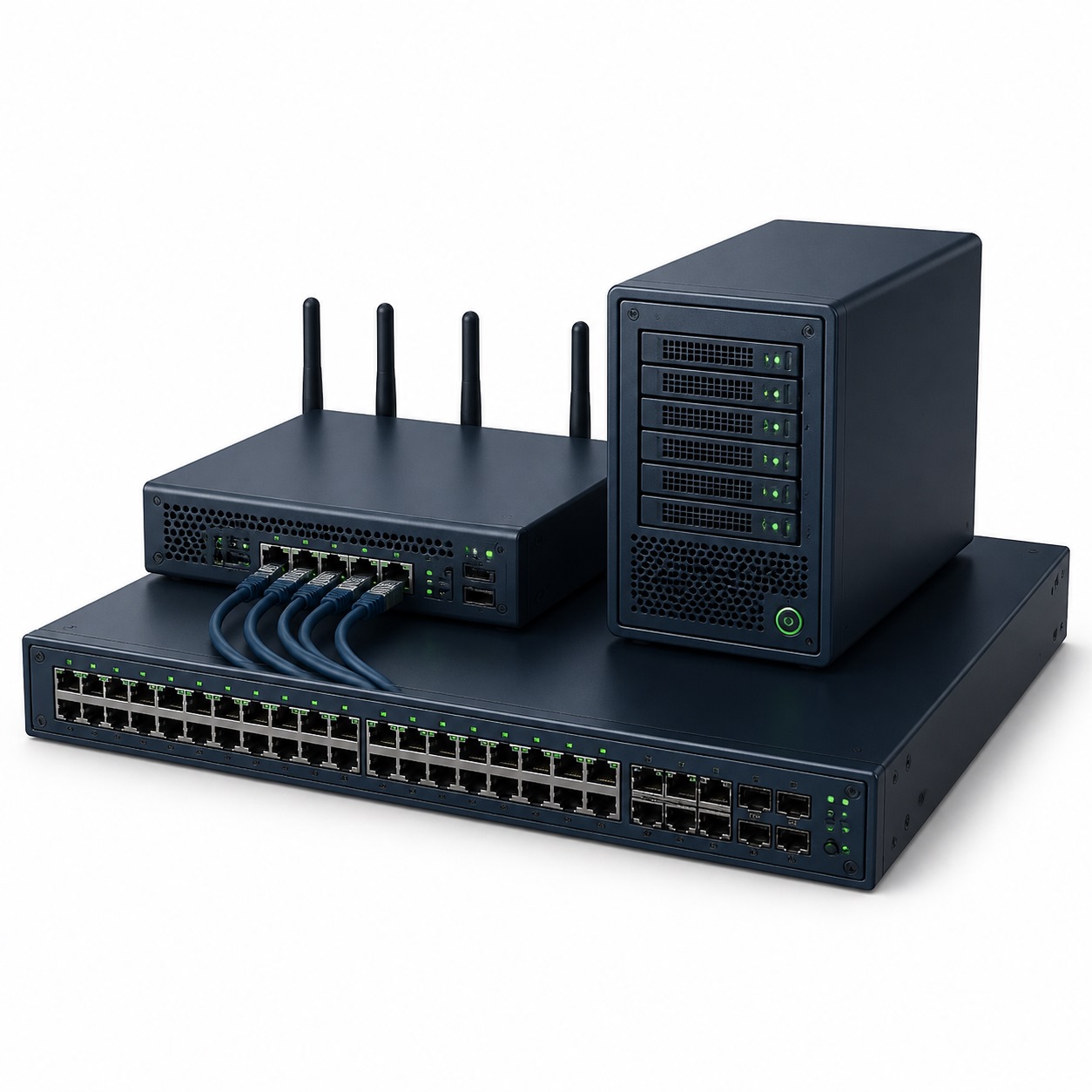 Telecommunications
The PDF lists routers, switches and servers. Use the RTC for local calendar retention and management logs, not as a replacement for network synchronization or a standards-traceable time source.
Telecommunications
The PDF lists routers, switches and servers. Use the RTC for local calendar retention and management logs, not as a replacement for network synchronization or a standards-traceable time source.
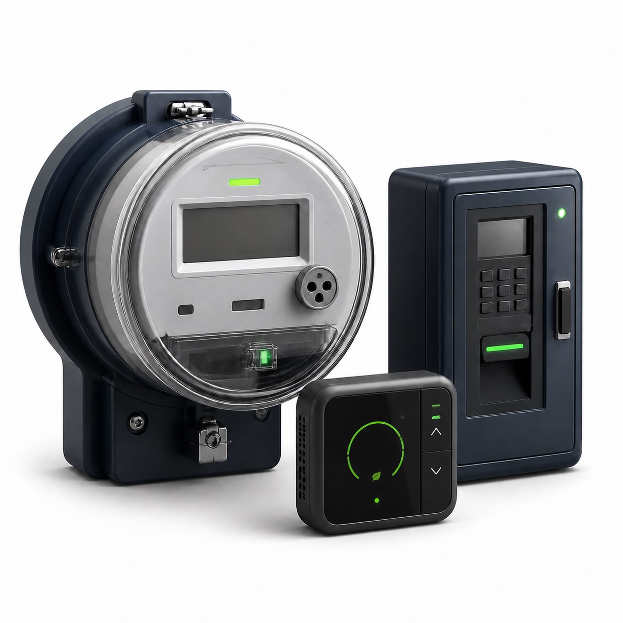 Utility and Other Equipment
The PDF lists utility meters, vending machines, thermostats and modems. Transaction data and control history must be stored outside the RTC, and firmware must reject timestamps until time validity is established.
Utility and Other Equipment
The PDF lists utility meters, vending machines, thermostats and modems. Transaction data and control history must be stored outside the RTC, and firmware must reject timestamps until time validity is established.
FRTC1338S Engineering FAQs
What is the FRTC1338S?
FRTC1338S is a NYFEA I²C real-time clock device. FRTC1338S combines BCD timekeeping and 56 bytes of NV SRAM. The recommended VCC table specifies 2.97 V to 3.63 V; the page therefore does not generalize the feature-page reference to 1.8 V operation as a guaranteed VCC range.
What supply range does FRTC1338S use?
The controlled PDF specifies VCC 2.97 V to 3.63 V. The timekeeping or backup condition is listed separately as VBAT 1.3 V to 3.7 V in the recommended-condition table.
Does FRTC1338S include a crystal?
External 32.768 kHz crystal; isolate the crystal network from RF and fast digital signals.
What is the FRTC1338S operating temperature range?
The supported operating range used on this page is -40 °C to +85 °C.
Can FRTC1338S replace another RTC without redesign?
Do not infer a drop-in replacement from a similar function, interface or package. Verify pinout, I²C address, register map, power-fail behavior, oscillator network, interrupt handling, package dimensions and firmware in the final system.
How should time validity be checked after power-up?
Initialize the device as required, inspect the available oscillator-stop or voltage-status flags, perform a coherent calendar read and reject timestamps until the system has established a valid time source.
This page summarizes the FRTC1338S product specification for product evaluation and engineering reference. It does not replace the complete controlled specification. Confirm the current revision, register definitions, pin configuration, interface timing, absolute maximum ratings, oscillator and backup requirements, package dimensions, PCB layout, assembly process and qualification requirements before production release.
Download FRTC1338S Product SpecificationContact NYFEA for Product Support