
FRTC4100S I²C Real-Time Clock with Battery Switchover and Software Calibration
NYFEA FRTC4100S is a low-power I²C real-time clock with BCD calendar counters, automatic battery switchover, software clock calibration and an open-drain frequency-test/output pin.
Product scope: FRTC4100S uses an external 32.768 kHz crystal; the stated 12.5 pF load capacitance is integrated in the oscillator circuit. The device maintains time from VBAT after switchover, but host access is disabled in backup mode.
Use the current controlled PDF for register definitions, timing, test conditions, switchover limits, package dimensions and production-release decisions.
Product Overview and Scope
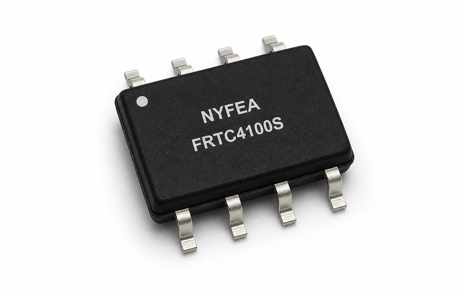
FRTC4100S combines a crystal-controlled 32.768 kHz oscillator, calendar counters, an I²C serial interface, backup-power switching and software calibration in an SOP-8 package. The first eight register bytes contain the clock/calendar and control information in binary-coded decimal where specified.
Selection boundary: The external crystal, backup element, I²C pull-ups, power-transition behavior, firmware initialization and calibration process are part of the finished design. Similar address, function or package does not establish drop-in compatibility with another RTC.
Key Features
Calendar
Seconds, minutes, hours, day, date, month, year and century counters with automatic leap-year compensation.
Backup Operation
Automatic switchover to VBAT and bus deselection when VCC falls below the power-sense threshold.
Software Calibration
Programmable counter correction for measured crystal error under defined conditions.
FT/OUT
Open-drain pin for 512 Hz frequency testing or software-controlled output.
- I²C operation supports Standard-mode and Fast-mode timing up to 400 kHz.
- Typical battery current is 0.4 µA at 25 °C with VBAT = 3 V, VCC = 0 V and the oscillator running; the listed maximum is 1 µA under that condition.
- Operating ambient temperature is -40 °C to +85 °C; Pb-free SOP-8 package pitch is 1.27 mm.
Function Block
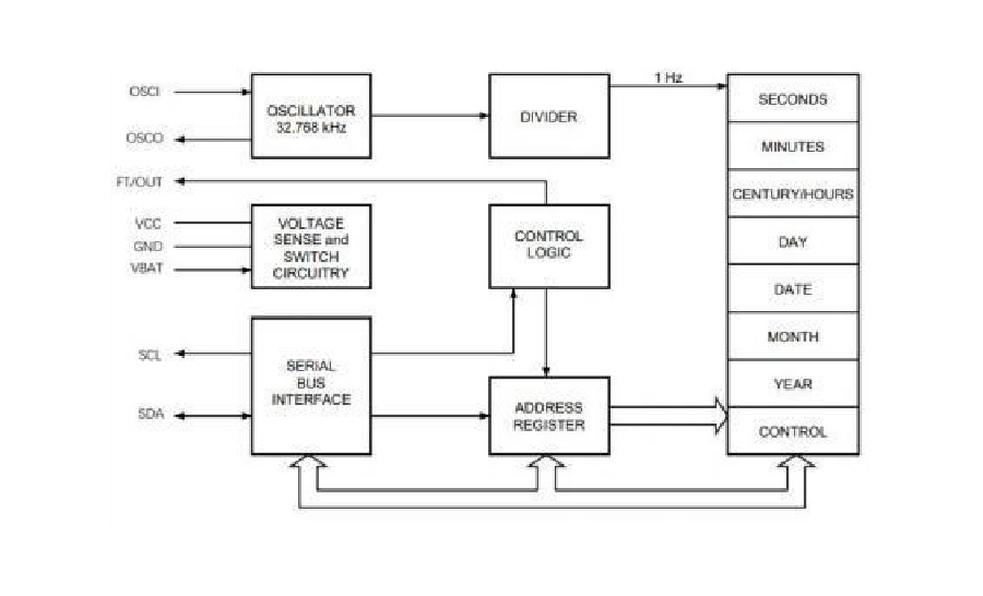
The oscillator and divider generate the 1 Hz calendar time base. Voltage-sense circuitry manages source selection, the serial interface transfers register data, and the control logic operates the calibration and FT/OUT functions.
Timekeeping, Calendar and Startup Behavior
Clock/calendar data occupies register addresses 0 through 6; address 7 contains the calibration and control bits. Firmware must preserve reserved bits and apply the register-specific BCD field definitions.
| Address | Function | Engineering note |
|---|---|---|
| 0 | Seconds and ST | ST stops or starts the oscillator. For worst-case startup, the PDF recommends setting ST to 1 and then clearing it to 0. |
| 1 | Minutes | BCD minutes field. |
| 2 | Century / hours | Includes the century indication and hour data as defined by the register map. |
| 3–6 | Day, date, month and year | Apply valid ranges and automatic leap-year behavior defined in the PDF. |
| 7 | Calibration / control | Contains calibration sign and magnitude, FT and OUT control functions. |
Coherent read behavior: The PDF states that a clock update is delayed for 250 ms when a clock address is being read. This does not stop actual timekeeping; firmware should still complete a multi-byte calendar read promptly and validate the result.
At power-on, FT defaults to 0 and OUT defaults to 1; the PDF describes all other register bits as random. Production firmware must therefore initialize all required calendar and control fields before accepting timestamps.
I²C Interface, Read Mode and Write Mode
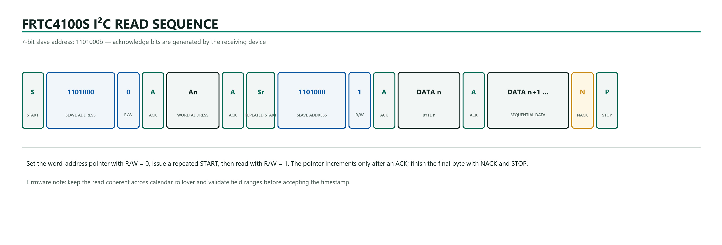
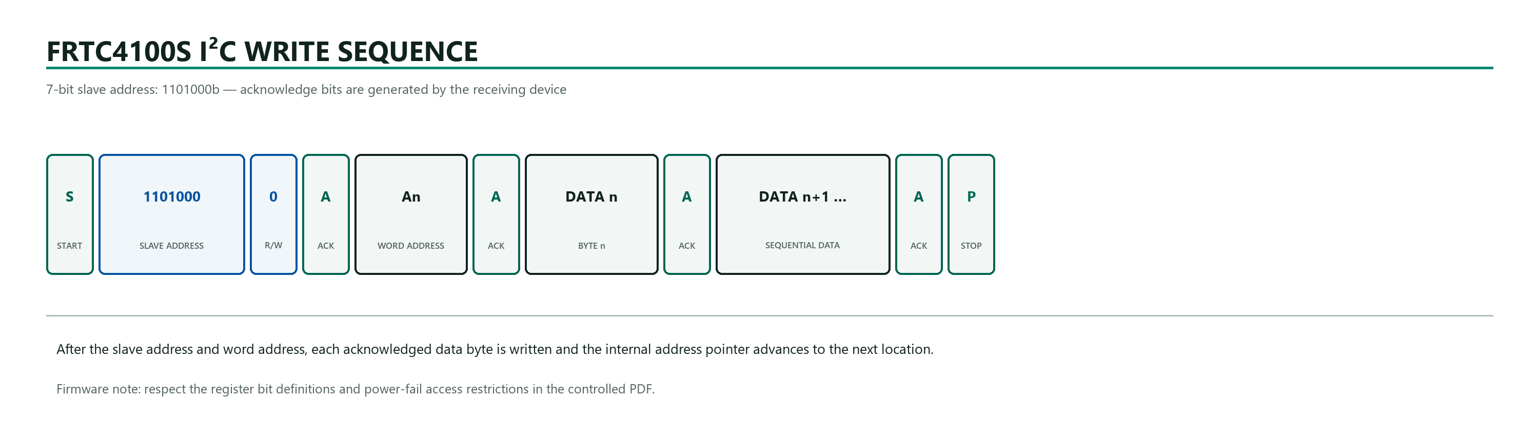
| 7-bit slave address | 1101000b (0x68), before the R/W bit is appended |
|---|---|
| Bus modes | Standard-mode at 100 kHz and Fast-mode from 100 kHz to 400 kHz under the listed timing conditions |
| External pull-ups | SDA and SCL require pull-up resistors; FT/OUT is also open drain and requires an external pull-up when used |
| Address pointer | Automatically advances through sequential acknowledged accesses |
Power, Backup Switchover and Data Validity
| Primary supply | VCC = 2.0 V to 5.5 V |
|---|---|
| Backup source | VBAT = 2.5 V minimum, 3.0 V typical and 3.5 V maximum in the recommended table; after switchover, the PDF permits a 2.0 V minimum for a crystal with RS = 40 kΩ |
| Switchover threshold | VSO is specified relative to VBAT: VBAT - 0.80 V minimum, VBAT - 0.50 V typical and VBAT - 0.30 V maximum |
| Battery current | 0.4 µA typical and 1 µA maximum at 25 °C, VBAT = 3 V, VCC = 0 V, oscillator running |
| Bus access in backup | When VCC falls below VSO, access terminates, the address counter resets and bus inputs are ignored while timekeeping continues from VBAT |
| VCC fall rate | Must not exceed 5 mV/µs under the specification note |
The PDF gives a typical data-retention example exceeding five years with a 50 mAh, 3 V lithium cell. This is a conditional example, not a guaranteed finished-system lifetime; calculate service life using source derating, worst-case RTC current, leakage and environmental conditions.
3.3 V design note: The PDF warns that an initially high backup voltage can reduce switchover margin for a 3.3 V ±10% VCC rail. Verify worst-case VBAT, VCC tolerance and VSO before production release.
Electrical Conditions, Crystal and Calibration
| Operating temperature | -40 °C to +85 °C |
|---|---|
| Crystal | 32.768 kHz; CL = 12.5 pF; series resistance up to 100 kΩ |
| Uncalibrated frequency error | The PDF states tested oscillator error does not exceed 35 ppm at 25 °C, approximately ±1.53 minutes per month |
| Calibrated accuracy statement | Better than ±2 ppm at 25 °C after correct measurement and programming |
| Calibration cycle | 64 minutes; positive and negative correction use different step sizes |
| Calibration step | Approximately +4.068 ppm per positive step or -2.034 ppm per negative step |
| Calibration range | 31 steps, stated as approximately +5.5 or -2.75 minutes per month |
| FT test output | 512 Hz when FT is enabled; open-drain output requires an external pull-up |
Accuracy boundary: The better-than-±2 ppm statement is conditional at 25 °C after calibration. It is not an uncalibrated full-temperature guarantee and does not remove crystal aging, temperature dependence, layout coupling or measurement uncertainty.
System Integration Guidance
The controlled PDF does not identify a normative “Typical Application Circuit.” The diagram below is an engineering integration guide that organizes the documented pins and external design responsibilities; it must not be interpreted as a guaranteed reference circuit.
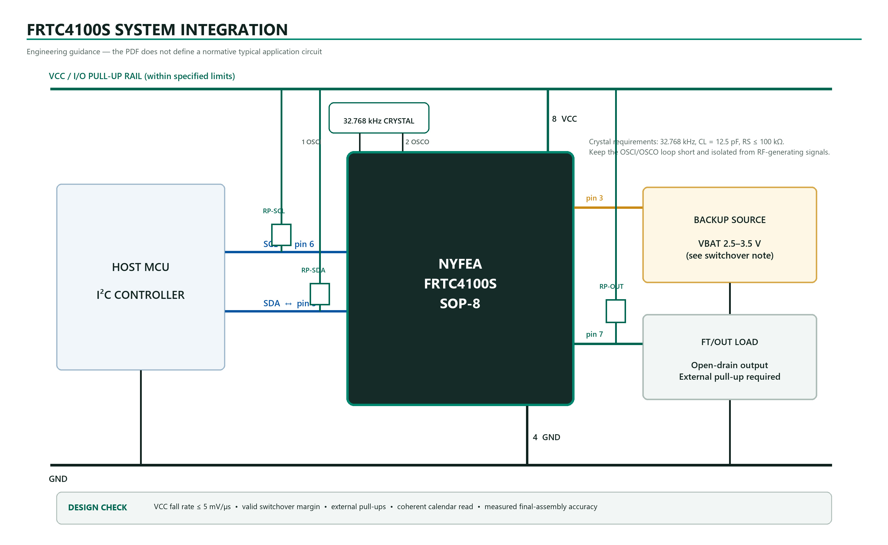
- Keep OSCI and OSCO traces as short as practicable and isolate the oscillator loop from RF-generating or fast-switching nets.
- Size SDA, SCL and FT/OUT pull-ups for the selected rail, bus capacitance, clock rate and sink-current limits.
- Measure the 512 Hz FT/OUT signal with calibrated equipment under defined conditions before calculating and programming a calibration code.
- Verify the assembled product through VCC loss and recovery, including deselection, time retention, bus recovery and timestamp validity.
Package Information
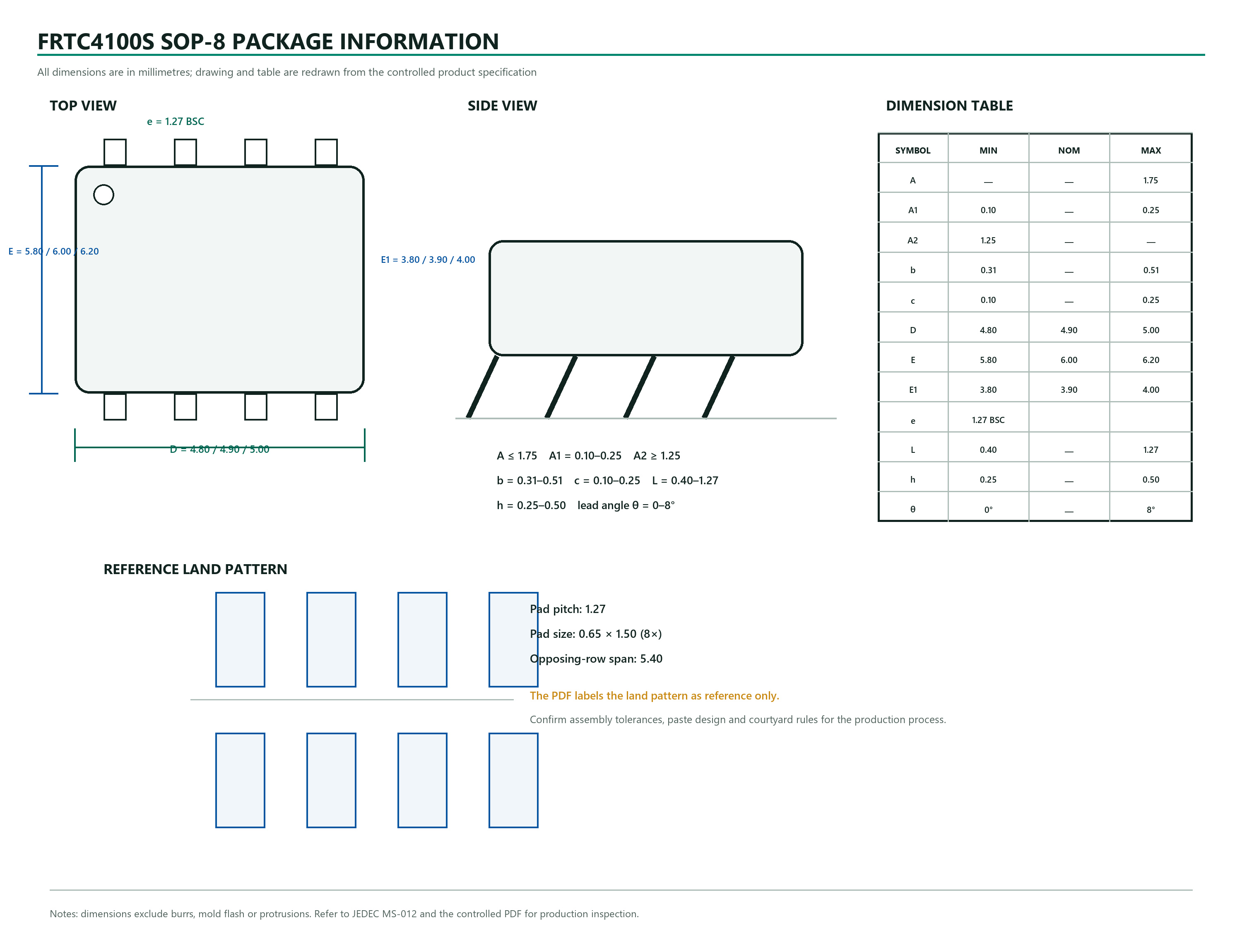
Available package: SOP-8 with 1.27 mm lead pitch. The product appearance image is illustrative and must not be used for terminal numbering, dimensional inspection or land-pattern design.
Application Guidance and Design Limitations
The FRTC4100S product specification does not publish a target-application list. The following are engineering evaluation contexts derived from the documented calendar, backup-switchover, programmable-output and calibration functions; they are not manufacturer application claims.
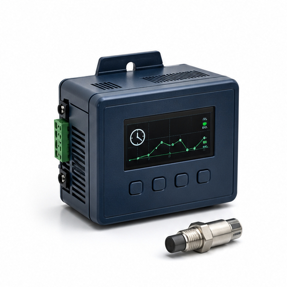 Event Logging and TimestampingEvaluate retained calendar time for local records in data loggers and monitoring equipment. Event storage, traceability and external time synchronization remain host-system responsibilities.
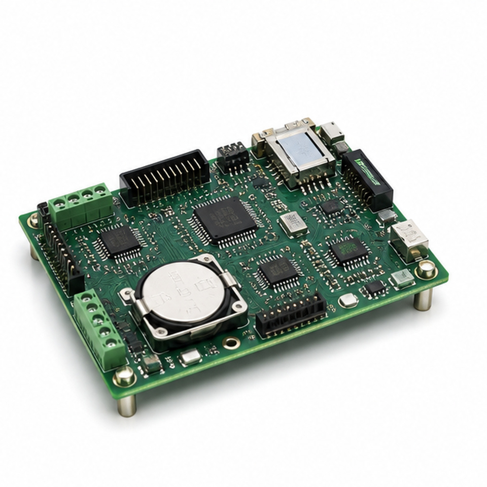 Battery-Backed Embedded ControllersUse automatic source switching where calendar time must continue after VCC loss. Qualify backup voltage, leakage, source impedance, service life and access recovery.
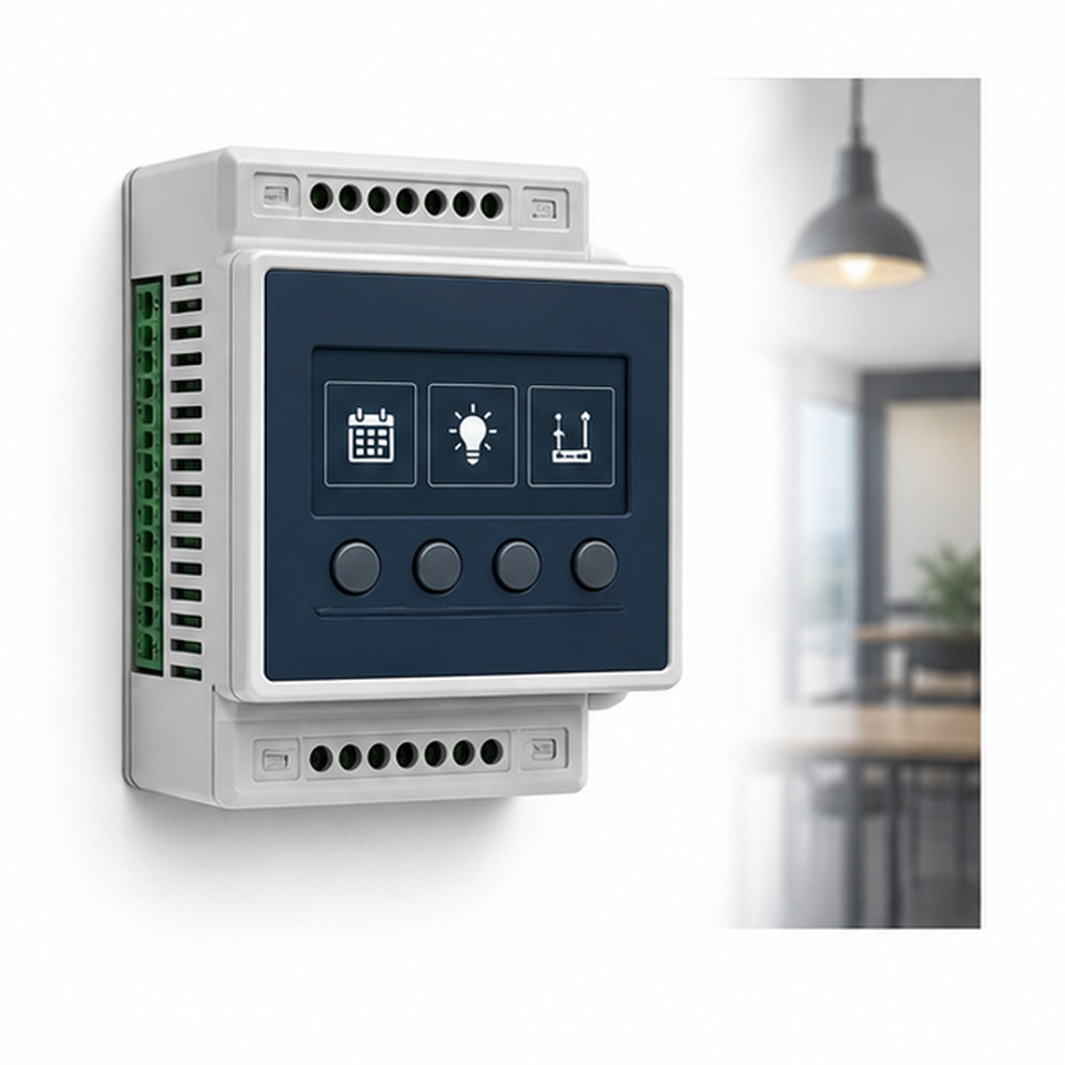 Scheduled Control EquipmentCalendar counters and programmable output can support local scheduled functions. The host must define fail-safe behavior and revalidate time before acting after power restoration.
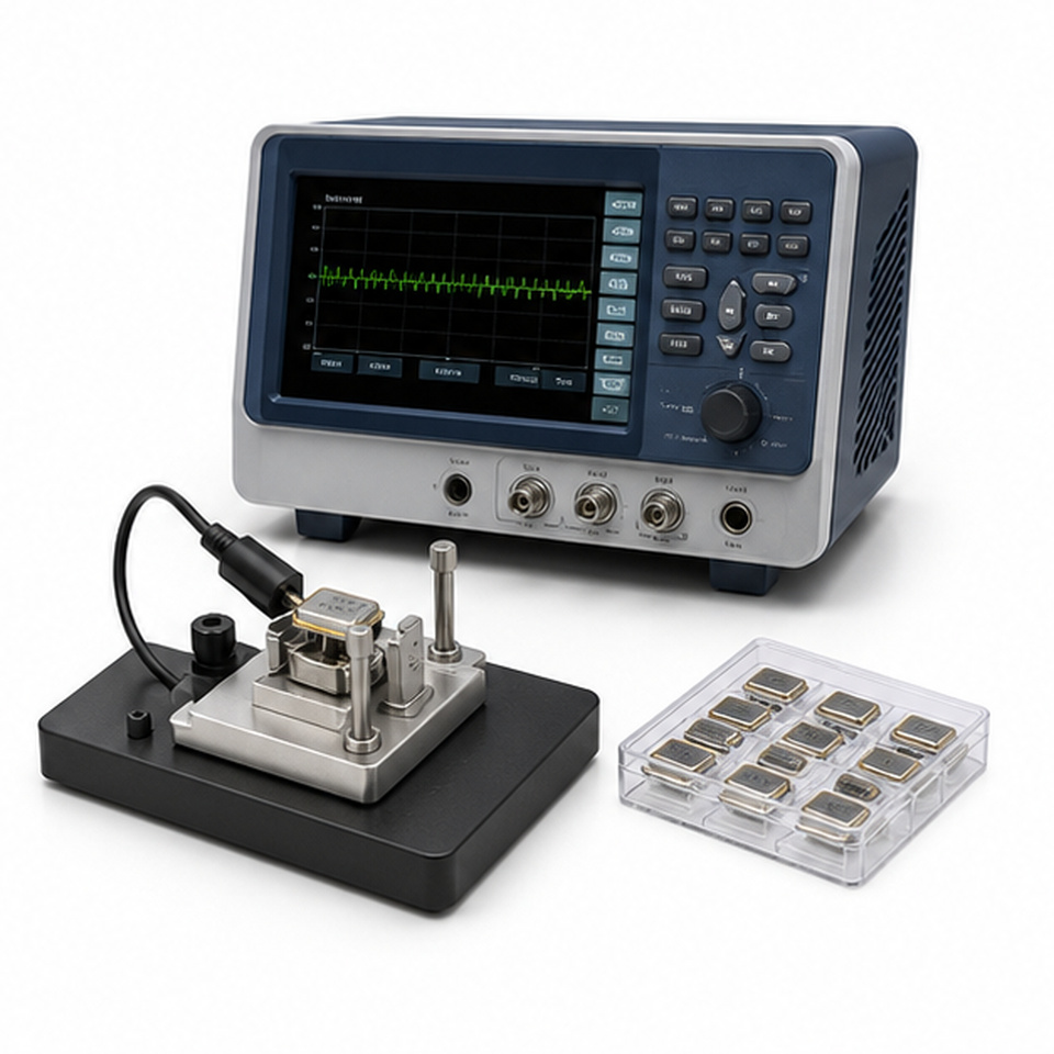 Production Clock CalibrationUse FT/OUT and software correction where measured final-assembly accuracy is required. Define the reference instrument, test temperature, fixture, code calculation and production limits.
Application boundary: Validate clock accuracy, initialization, backup life, I²C operation, source switching, EMC, assembly, safety and environmental performance in the finished product. These examples are not application certification or a guarantee of system performance.
FRTC4100S Engineering FAQs
What is the FRTC4100S?
FRTC4100S is a low-power I²C real-time clock with BCD calendar counters, automatic battery switchover, software clock calibration and an open-drain FT/OUT pin. It uses an external 32.768 kHz crystal.
Does FRTC4100S include a 32.768 kHz crystal?
No. FRTC4100S integrates the 12.5 pF oscillator load capacitance, but the 32.768 kHz crystal is external. The PDF lists crystal series resistance up to 100 kΩ and requires short, quiet OSCI and OSCO routing.
What is the FRTC4100S I²C slave address?
The controlled specification shows the 7-bit address as 1101000b, equivalent to 0x68 before the R/W bit is appended.
How is a sequential read performed?
Write the word address with R/W = 0, issue a repeated START, address the device with R/W = 1 and read sequential bytes. The pointer advances when the receiver acknowledges a byte; terminate the final byte with NACK and STOP.
What does the better-than-±2 ppm calibration statement mean?
Software calibration can improve accuracy to better than ±2 ppm at 25 °C when oscillator error is correctly measured and programmed. It is not an uncalibrated full-temperature guarantee and does not eliminate crystal or temperature drift.
Can the host access FRTC4100S while it is powered from VBAT?
No. When VCC falls below the switchover threshold, access terminates, the address counter resets and bus inputs are ignored while timekeeping continues from the backup source.
What should be checked in a 3.3 V switchover design?
Use the VSO limits relative to VBAT and the PDF's 3.3 V application note. An initially high backup voltage can reduce margin and may cause unintended switchover or deselection; verify worst-case source tolerances and VCC fall rate.
Can FRTC4100S directly replace another 0x68 SOP-8 RTC?
Not from address or package alone. Compare terminal assignment, register map, oscillator and calibration method, backup thresholds, power-fail access behavior, timing, FT/OUT function and package dimensions before migration.
This page summarizes the FRTC4100S product specification for product evaluation and engineering reference. It does not replace the complete controlled specification. Confirm the current revision, register definitions, pin configuration, interface timing, absolute maximum ratings, oscillator and backup requirements, package dimensions, PCB layout, assembly process and qualification requirements before production release.
Download FRTC4100S Product SpecificationContact NYFEA for Product Support