
FRTC4111S I²C RTC with 56-Byte Battery-Backed NVRAM
NYFEA FRTC4111S is a low-power I²C real-time clock that combines BCD calendar counters, 56 bytes of battery-backed general-purpose RAM, automatic power switchover and software calibration.
Product scope: FRTC4111S uses an external 32.768 kHz crystal. The clock and RAM are retained from VBAT after switchover, but I²C access is disabled in backup mode. External pull-ups, bypass capacitors, backup-source sizing, initialization and accuracy verification remain system-design responsibilities.
Use the current controlled PDF for register definitions, timing, test conditions, switchover limits, package dimensions and production-release decisions.
Product Overview and Scope
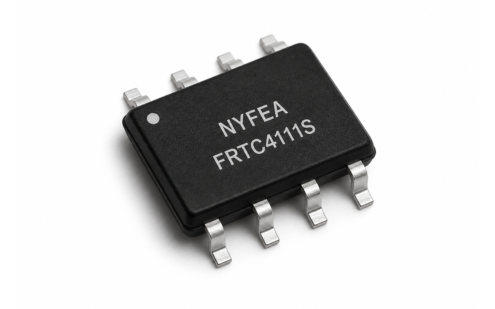
FRTC4111S integrates a crystal-controlled calendar RTC, I²C serial interface, automatic backup-power switching, software calibration and 56 bytes of general-purpose RAM in an SOP-8 package. The first eight addresses contain clock, calendar and control registers; addresses 0x08 through 0x3F provide battery-backed RAM.
Selection boundary: The RAM is general-purpose storage, not nonvolatile memory independent of VBAT. Similar address, package or calendar function does not establish drop-in compatibility with another RTC.
Key Features
Calendar
Seconds, minutes, hours, day, date, month, year and century counters with automatic leap-year compensation.
56-Byte RAM
General-purpose addresses 0x08–0x3F are retained together with timekeeping while the valid backup source is present.
Backup Operation
Automatic VCC-to-VBAT switchover and I²C deselection protect retained state during primary-power loss.
Calibration and FT/OUT
Software correction and an open-drain 512 Hz test/software output support measured production calibration.
- Standard-mode and Fast-mode I²C operation up to 400 kHz.
- Typical battery current is 0.4 µA at 25 °C with VBAT = 3 V, VCC = 0 V and the oscillator running; listed maximum is 1 µA.
- SOP-8 package with 1.27 mm pitch; operating ambient temperature -40 °C to +85 °C.
Function Block
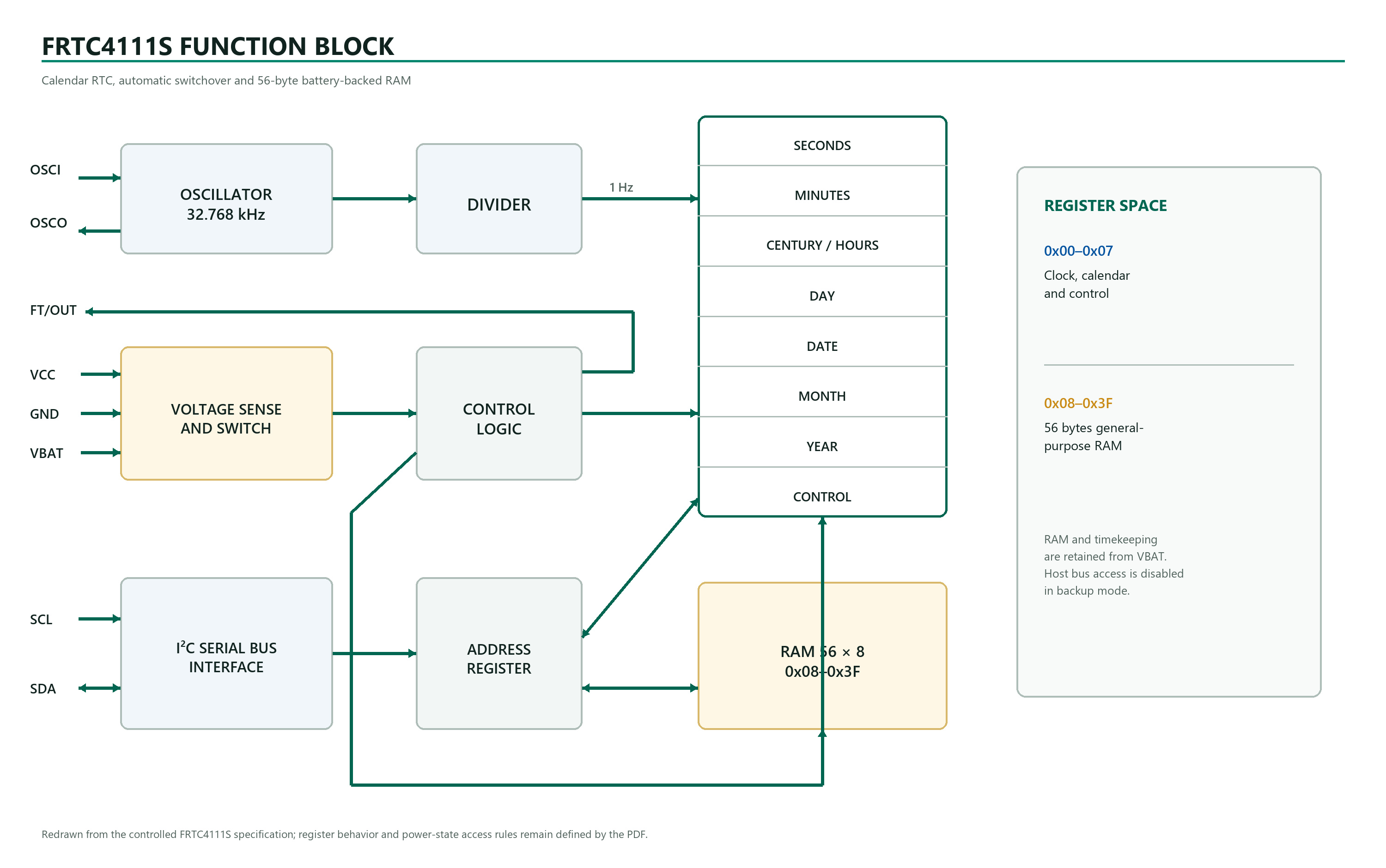
The oscillator and divider create the 1 Hz time base. Calendar/control registers and 56-byte RAM share the serial address space, while voltage-sense circuitry controls source selection and I²C availability.
Timekeeping, Calendar, RAM and Startup
The complete sequential address space contains 64 bytes. Firmware must preserve reserved bits, apply the register-specific BCD definitions and distinguish retained RAM from clock/control registers.
| Address | Function | Engineering note |
|---|---|---|
| 0x00 | Seconds and ST | Use the specified ST kick-start sequence after initial power-up. |
| 0x01–0x06 | Minutes through year | BCD calendar fields with defined ranges and century/leap-year behavior. |
| 0x07 | Control | OUT, FT, calibration sign and magnitude. |
| 0x08–0x3F | 56-byte RAM | Battery-backed general-purpose data; unavailable to the host while the device is in backup mode. |
Coherent read behavior: A clock update is delayed for 250 ms while a clock address is read. Actual timekeeping continues; complete multi-byte reads promptly and validate field ranges.
At power-on, FT defaults to 0 and OUT defaults to 1; other bits are described as random. Initialize all required clock, control and application-owned RAM data before accepting timestamps or stored state.
I²C Interface, Read Mode and Write Mode
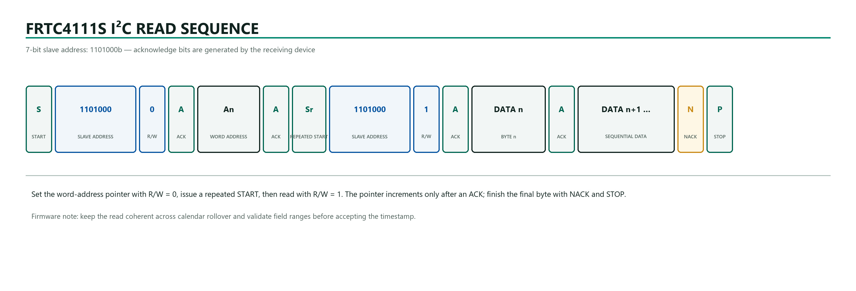
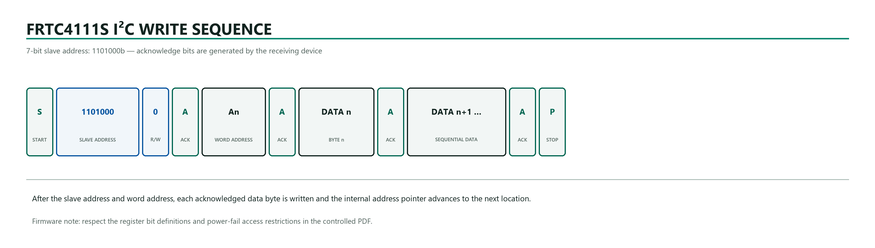
| 7-bit slave address | 1101000b (0x68), before the R/W bit is appended |
|---|---|
| Bus modes | Standard-mode at 100 kHz and Fast-mode from 100 kHz to 400 kHz under the listed timing conditions |
| External pull-ups | SDA and SCL require pull-up resistors; FT/OUT is also open drain and requires an external pull-up when used |
| Address pointer | Automatically advances through sequential acknowledged accesses |
Power, Backup Switchover and Data Validity
| Primary supply | VCC = 2.0 V to 5.5 V |
|---|---|
| Backup source | VBAT = 2.5 V minimum, 3.0 V typical and 3.5 V maximum; after switchover, the PDF permits 2.0 V minimum with a 40 kΩ crystal series resistance |
| Switchover threshold | The table specifies VSO minimum as VBAT - 0.80 V; do not assume typical or maximum values not stated in this PDF |
| Battery current | 0.4 µA typical and 1 µA maximum at 25 °C, VBAT = 3 V, VCC = 0 V, oscillator running |
| Backup behavior | Clock and RAM are retained; I²C inputs are not recognized and host reads/writes are unavailable |
| Recovery / fall rate | tREC = 10 µs; VCC fall rate must not exceed 5 mV/µs under the stated condition |
The PDF gives a typical retention example exceeding five years with a 50 mAh, 3 V lithium cell. Treat it as an illustrative calculation, not a guaranteed service life; include cell derating, leakage, worst-case RTC current and environmental effects.
3.3 V design note: If the initial backup-source voltage is at or above a 3.3 V VCC rail, the PDF warns that source voltage may need to be reduced. Verify worst-case VCC, VBAT and VSO margin.
Electrical Conditions, Crystal and Calibration
| Operating temperature | -40 °C to +85 °C |
|---|---|
| Crystal | 32.768 kHz; CL = 12.5 pF; series resistance up to 100 kΩ |
| Uncalibrated frequency error | The PDF states tested oscillator error does not exceed 35 ppm at 25 °C, approximately ±1.53 minutes per month |
| Calibrated accuracy statement | Better than ±2 ppm at 25 °C after correct measurement and programming |
| Calibration cycle | 64 minutes; positive and negative correction use different step sizes |
| Calibration step | Approximately +4.068 ppm per positive step or -2.034 ppm per negative step |
| Calibration range | 31 steps, stated as approximately +5.5 or -2.75 minutes per month |
| FT test output | 512 Hz when FT is enabled; open-drain output requires an external pull-up |
Accuracy boundary: The better-than-±2 ppm statement is conditional at 25 °C after calibration. It is not an uncalibrated full-temperature guarantee and does not remove crystal aging, temperature dependence, layout coupling or measurement uncertainty.
Typical Application Circuit
The PDF defines a representative circuit with 4.7 kΩ SCL/SDA pull-ups, a 10 kΩ FT/OUT pull-up, 0.1 µF and 4.7 µF VCC bypass capacitors, a 0.1 µF VBAT capacitor and an external 32.768 kHz crystal.
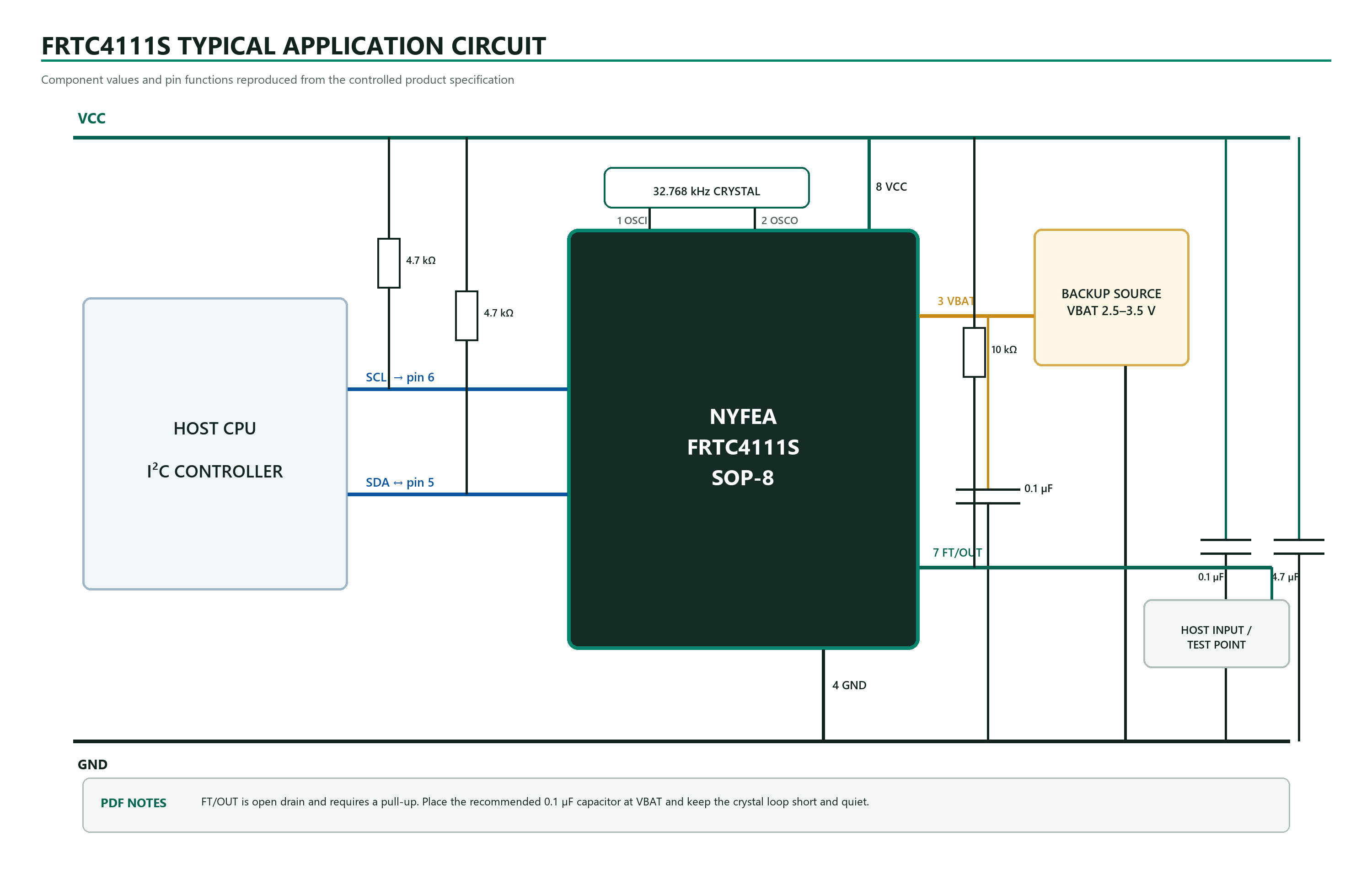
- Place the 0.1 µF VBAT capacitor close to pin 3 and the VCC bypass components close to pin 8 and ground.
- Keep the OSCI/OSCO loop short and isolated from RF-generating or fast-switching nets.
- FT/OUT is open drain; use the external pull-up shown when the output is required.
- Validate source switching, retained RAM, bus recovery and clock accuracy in the assembled product.
Package Information
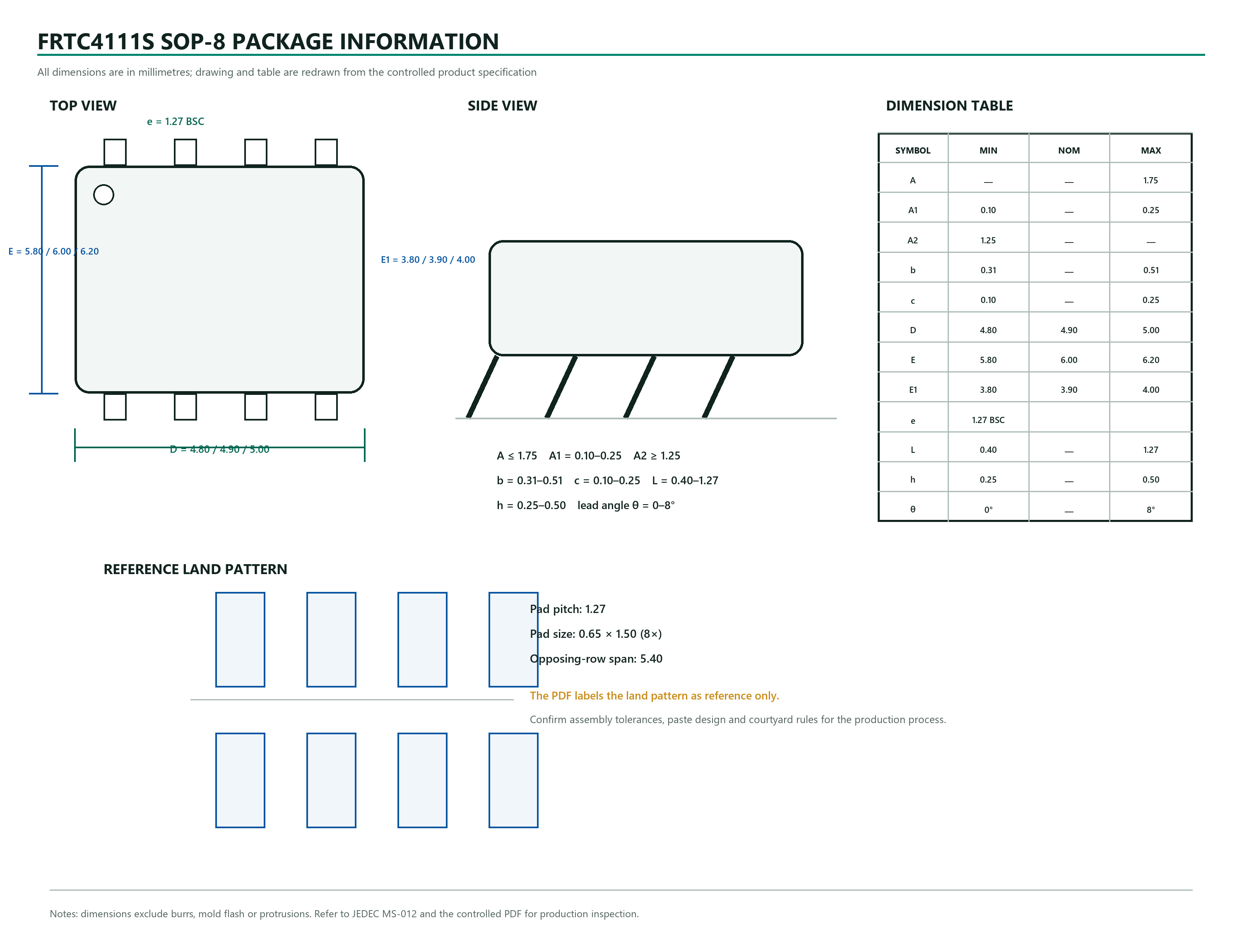
Available package: SOP-8 with 1.27 mm lead pitch. The product appearance image is illustrative and must not be used for terminal numbering, dimensional inspection or land-pattern design.
Application Guidance and Design Limitations
The product specification explicitly lists portable instruments, electronic metering, battery-powered products and telecom equipment. The examples below translate those categories into engineering evaluation contexts; they do not represent application certification.
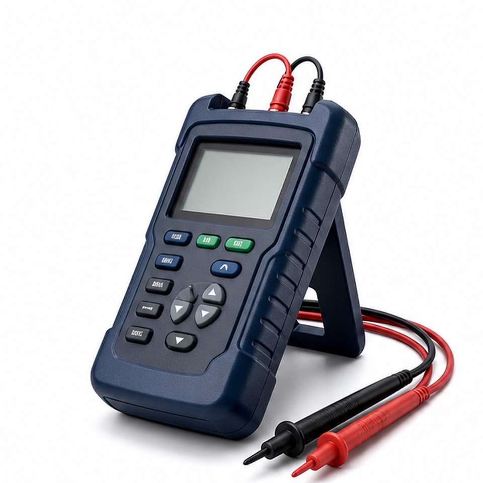 Portable InstrumentsRetain clock and compact application state across main-power interruptions. Verify backup life, timestamp validity and recovery behavior.
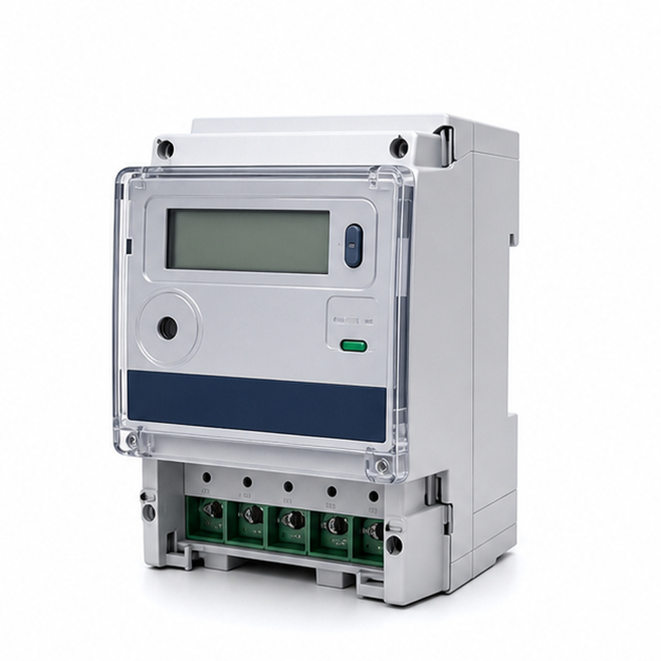 Electronic MeteringUse calendar time and retained RAM for local records where permitted. Metrology, legal-time and data-integrity requirements remain system responsibilities.
 Battery-Powered ProductsEvaluate the 0.4 µA typical backup-current condition against cell derating, leakage, source impedance and required service life.
 Telecom EquipmentSupport local timestamps and retained configuration state. Define external synchronization, fault recovery and data-validity rules in the host system.
Application boundary: Validate clock accuracy, initialization, backup retention, RAM integrity, I²C operation, EMC, assembly, safety and environmental performance in the finished product.
FRTC4111S Engineering FAQs
What is the FRTC4111S?
FRTC4111S is a low-power I2C real-time clock with BCD calendar counters, 56 bytes of battery-backed general-purpose RAM, automatic battery switchover, software calibration and an open-drain FT/OUT pin.
How much battery-backed RAM does FRTC4111S provide?
The address map assigns 56 bytes of general-purpose RAM to addresses 0x08 through 0x3F. The RAM and timekeeping state are retained from VBAT, but host bus access is disabled in backup mode.
Does FRTC4111S include a 32.768 kHz crystal?
No. The crystal is external. The specification lists 32.768 kHz, 12.5 pF load capacitance and crystal series resistance up to 100 kΩ; keep the oscillator loop short and quiet.
What is the FRTC4111S I2C address?
The PDF shows D0h as the 8-bit write address. The corresponding 7-bit slave address is 0x68 before the read/write bit is appended.
Can the host access the clock or RAM while FRTC4111S is on VBAT?
No. When VCC falls below the switchover threshold, the device maintains the clock and RAM from VBAT but does not recognize I2C inputs.
How should FRTC4111S be initialized after power-up?
The specification recommends setting the ST bit to 1 and then clearing it to 0 to start the oscillator. FT defaults to 0 and OUT defaults to 1; other register values are described as random, so firmware should initialize all required registers.
What does better than ±2 ppm calibration mean?
The statement applies at 25 °C after oscillator error is measured and a suitable software-calibration code is programmed. It is not an uncalibrated full-temperature accuracy guarantee.
Can FRTC4111S directly replace another 0x68 SOP-8 RTC?
Not from address and package alone. Compare pinout, register map, NVRAM behavior, backup thresholds, power-fail access, oscillator, calibration, timing and FT/OUT behavior before migration.
This page summarizes the FRTC4111S product specification for product evaluation and engineering reference. It does not replace the controlled specification. Confirm the current revision, register definitions, pin configuration, interface timing, absolute maximum ratings, oscillator and backup requirements, package dimensions, PCB layout, assembly process and qualification requirements before production release.
Download FRTC4111S Product SpecificationContact NYFEA for Product Support