
FRTC8025S High-Stability I²C RTC with Integrated 32.768 kHz DTCXO
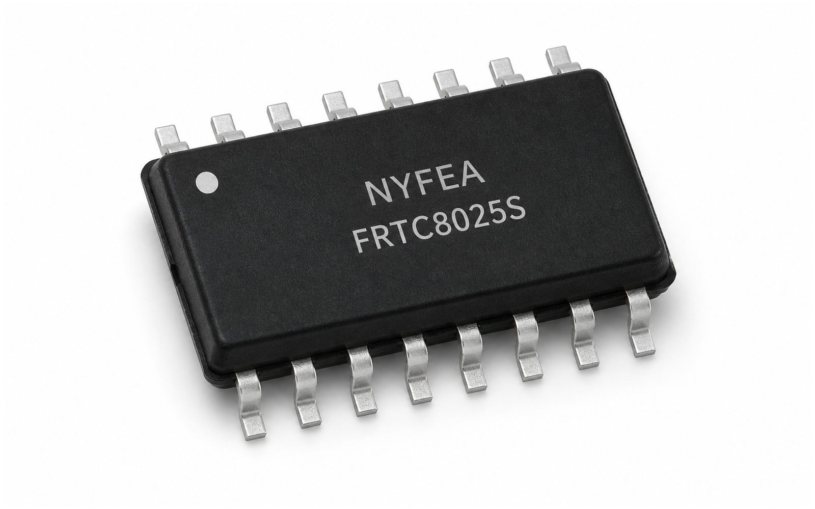
NYFEA FRTC8025S combines a temperature-compensated 32.768 kHz oscillator, calendar, alarm, fixed-cycle timer, update interrupt and selectable FOUT in one SOP-14 real-time clock module.
Product scope: The DTCXO and compensation data are integrated; no external tuning crystal is required. Published ppm values apply only with their adjacent VDD and temperature conditions. FRTC8025S has no dedicated VBAT pin, so backup design must maintain VDD within the applicable clock-retention conditions.
Use the current controlled PDF for register definitions, timing, test conditions, switchover limits, package dimensions and production-release decisions.
Product Overview and Scope
FRTC8025S is a high-stability I²C RTC module whose integrated DTCXO reduces external crystal selection and board-level oscillator tuning. It provides BCD calendar data, three interrupt classes, a temperature-compensated output and a readable temperature-data register.
Selection boundary: Integrated compensation reduces oscillator-component variation but does not remove supply, temperature, aging, measurement, firmware or complete-system validation requirements. Similar SOP-14 packaging does not imply compatibility.
Key Features
High-Stability DTCXO
Factory-programmed compensation data and on-chip temperature sensing support the stated frequency limits.
Calendar
Seconds through year in BCD with automatic leap-year correction from 2000 to 2099.
Three Interrupt Classes
Alarm, fixed-cycle timer and selectable second/minute update events share the open-drain /INT output.
Compensated FOUT
FOE-controlled CMOS output with selectable 32.768 kHz, 1024 Hz or 1 Hz operation.
- I²C Standard-mode and Fast-mode operation up to 400 kHz.
- Typical current is 0.54 µA at VDD = 3 V under the specified output-off condition.
- Operating ambient temperature is -40 °C to +85 °C.
Function Block
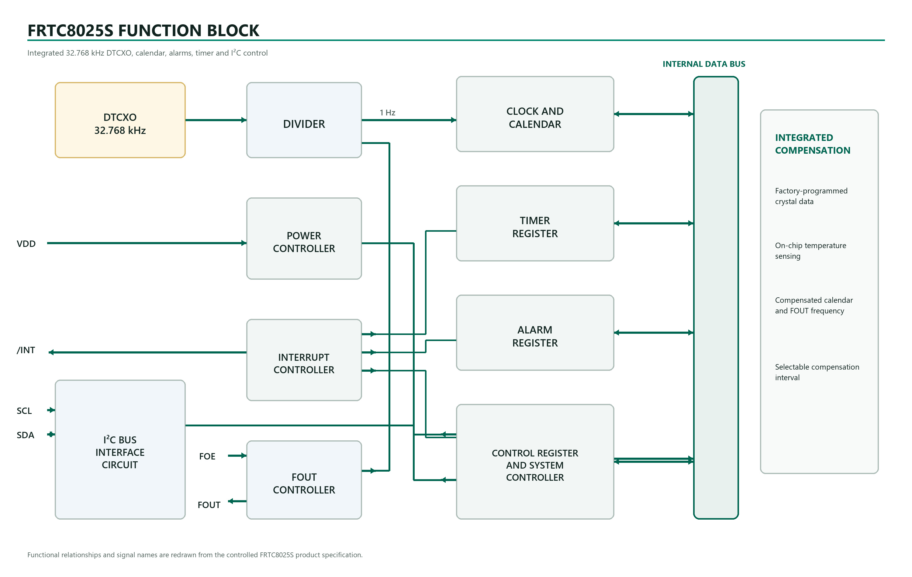
The integrated DTCXO feeds the divider and calendar. Alarm, timer and control registers share the internal bus, while dedicated controllers manage power, interrupts, FOUT and I²C access.
Calendar, Registers and Temperature Data
The RTC uses mirrored basic and extension register ranges. Write valid BCD calendar values, preserve mandatory-zero bits and reset or initialize all required registers after initial power-up or whenever VLF indicates uncertain data.
| Address | Function | Engineering note |
|---|---|---|
| 0x00–0x06 / 0x10–0x16 | Seconds through year | BCD calendar; week is one-hot. Leap-year handling covers 2000–2099. |
| 0x07 | 8-bit RAM | Dedicated read/write RAM byte. |
| 0x08–0x0A | Minute, hour, week/day alarm | May be used as RAM only when the alarm function is disabled as specified. |
| 0x0B–0x0C | Fixed-cycle timer counter | May be used as RAM only when the timer function is disabled as specified. |
| 0x0D–0x0F | Extension, flag and control | Contains timer source, FOUT selection, compensation interval, interrupt enables and RESET. |
| 0x17 | Temperature data | Updated during compensation; engineering conversion is (TEMP × 2 - 187.19) / 3.218 °C. |
Validity rule: VLF = 1 indicates that retained calendar or register data may be compromised. VDET = 1 indicates that temperature-compensation history may be compromised. Clear flags only according to the defined write-zero behavior.
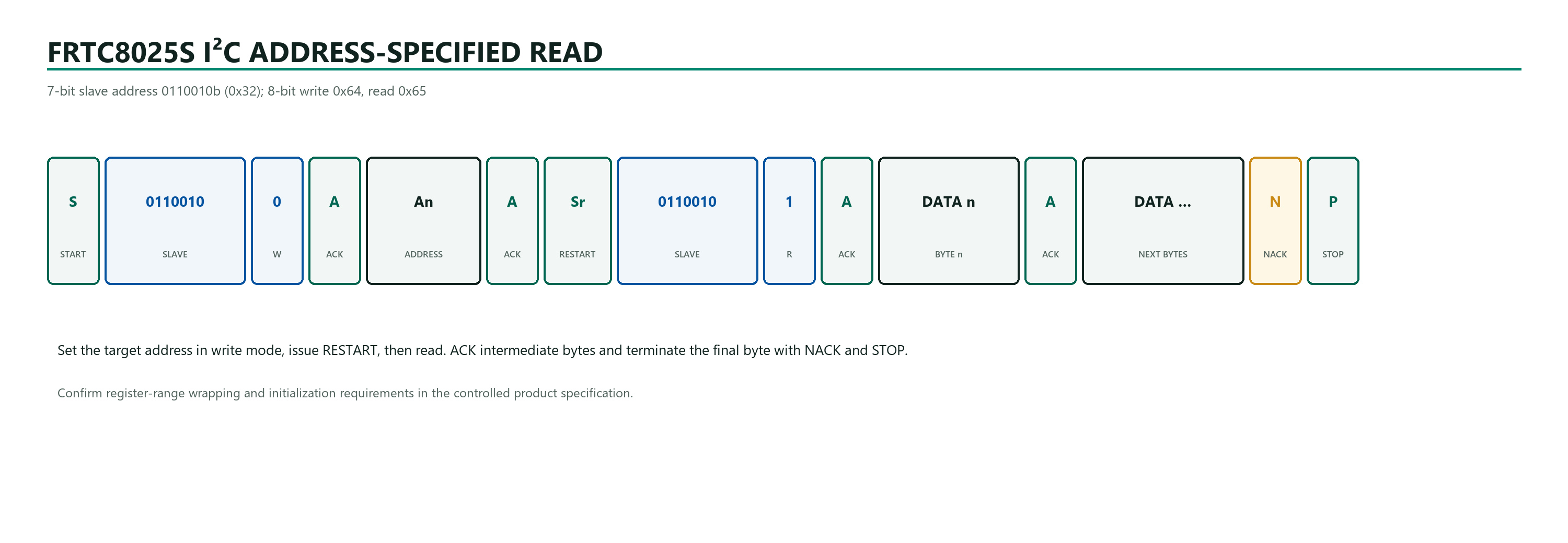
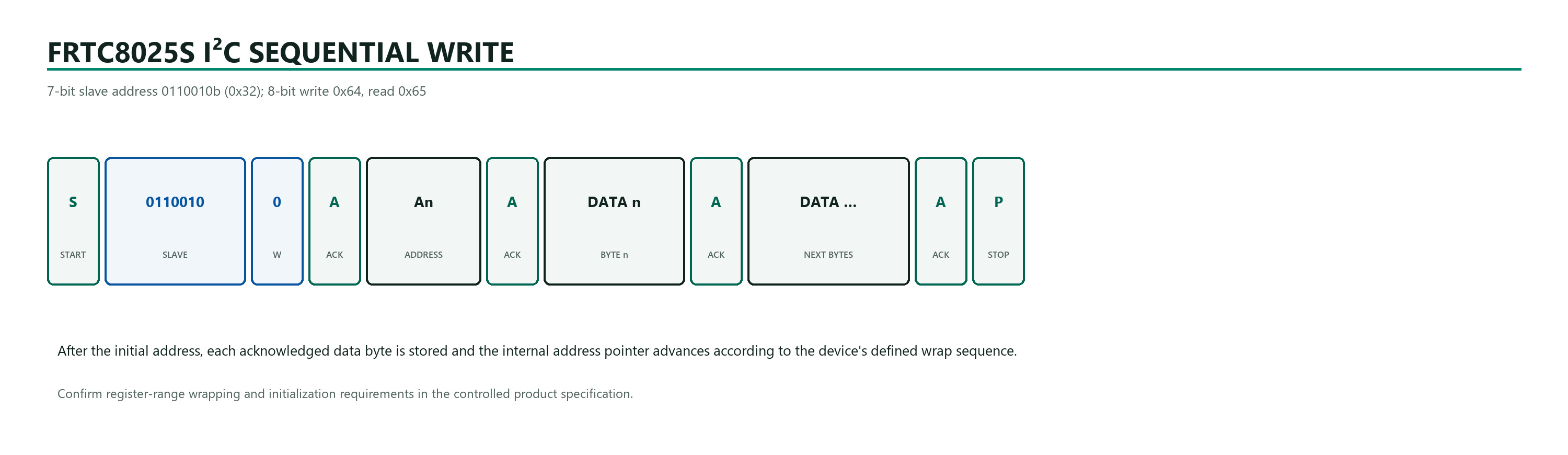
I²C Interface, Read Mode and Write Mode
| 7-bit slave address | 0110010b = 0x32 |
|---|---|
| 8-bit transfer address | 0x64 for write; 0x65 for read |
| Bus speed | Standard-mode at 100 kHz and Fast-mode up to 400 kHz |
| SDA | Open-drain during output; external pull-up required |
| Auto-increment | Address advances after each byte and wraps according to the basic or extension register range |
Power, Time Validity and Temperature Compensation
| Operating supply | VDD = 1.6 V to 5.5 V |
|---|---|
| Clock-retention voltage | VCLK = 1.15 V to 5.5 V; this is not the full-interface or compensation operating range |
| Backup architecture | No dedicated VBAT pin; maintain VDD from the selected backup source within the required conditions |
| Validity flags | VLF monitors clock/data reliability; VDET monitors temperature-compensation validity |
| Compensation intervals | 0.5 s, 2.0 s default, 10 s or 30 s; longer intervals reduce current but change compensation update behavior |
| Startup | Oscillation start time is specified up to 1.0 s at 25 °C and VDD 1.6–5.5 V |
Calculate backup life from the selected source, worst-case current, leakage, pull-up paths and required compensation behavior. A low enough voltage to retain the clock may be insufficient for valid temperature compensation or host communication.
Electrical and Frequency Characteristics
| Frequency precision | ±1.5 ppm at 0 °C to +50 °C and ±3.0 ppm at -40 °C to +85 °C; VDD = 3.0 V |
|---|---|
| Voltage characteristic | ±1.0 ppm/V maximum at 25 °C, VDD = 2.0 V to 5.5 V |
| First-year aging | ±3 ppm maximum at 25 °C, VDD = 3.0 V |
| Output off current, 3 V | 0.54 µA typical, 2.2 µA maximum under the stated compensation and interface conditions |
| FOUT active current, 3 V | 1.18 µA typical, 2.8 µA maximum with 32.768 kHz output and the stated conditions |
| Operating temperature | -40 °C to +85 °C |
| Storage temperature | -55 °C to +125 °C; this is an absolute-maximum stress range, not an operating condition |
Accuracy boundary: Do not present ±3 ppm as unconditional. It is specified at VDD = 3.0 V over the stated temperature range and remains subject to aging and the document's test method.
Typical Application and System Integration
The controlled PDF does not label a normative typical application circuit. The diagram below organizes the documented supply, I²C, /INT, FOE and FOUT connections and is therefore engineering guidance rather than a guaranteed reference design.
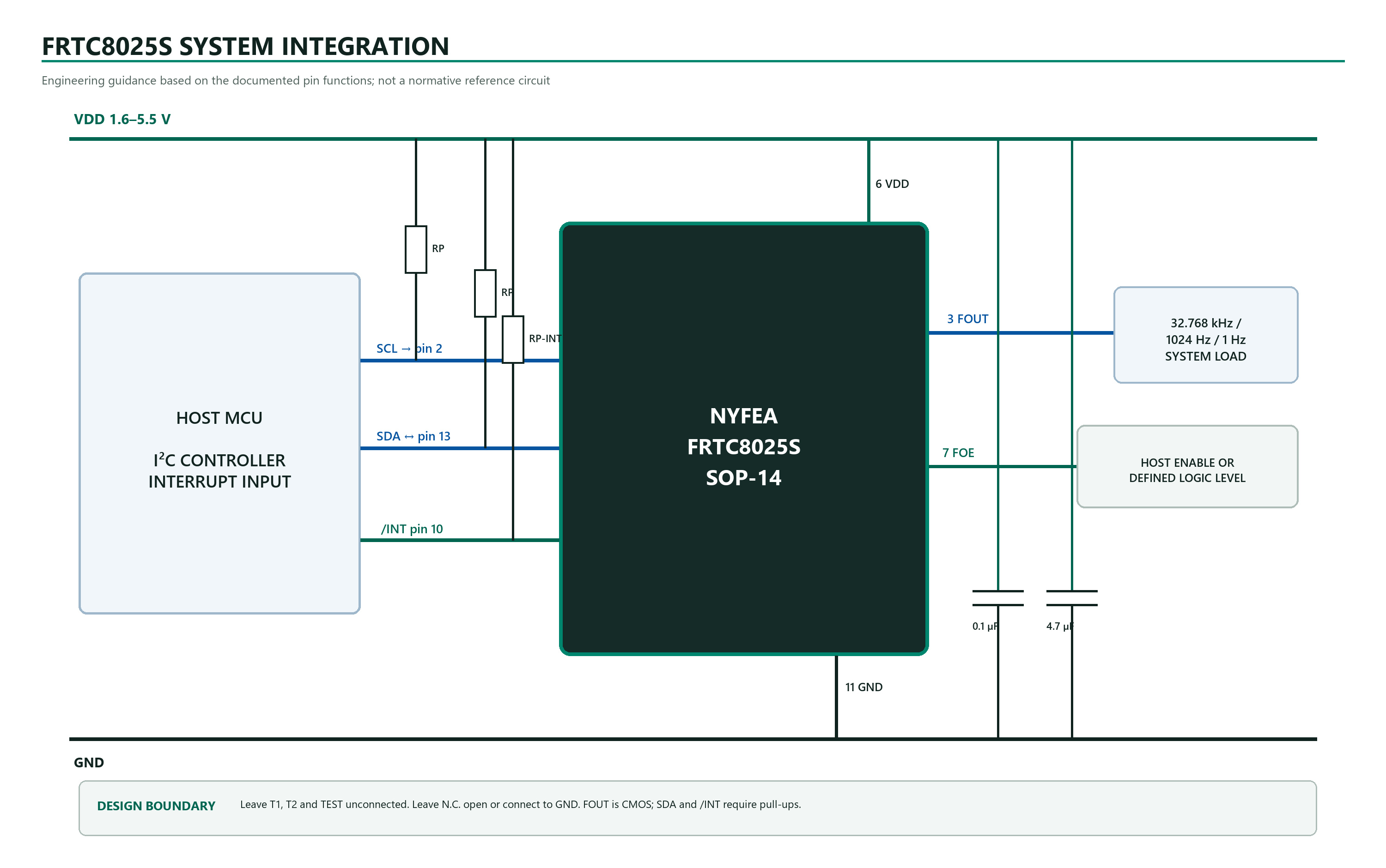
- Leave T1, T2 and TEST unconnected. Leave N.C. pins open or connect them to GND according to the pin guidance.
- SDA and /INT require pull-ups; FOUT is a CMOS output controlled by FOE.
- Maintain the supply conditions required for temperature compensation when the published ppm performance is needed.
- After a power event, inspect VLF and VDET before accepting time or compensated-frequency output as valid.
Package Information
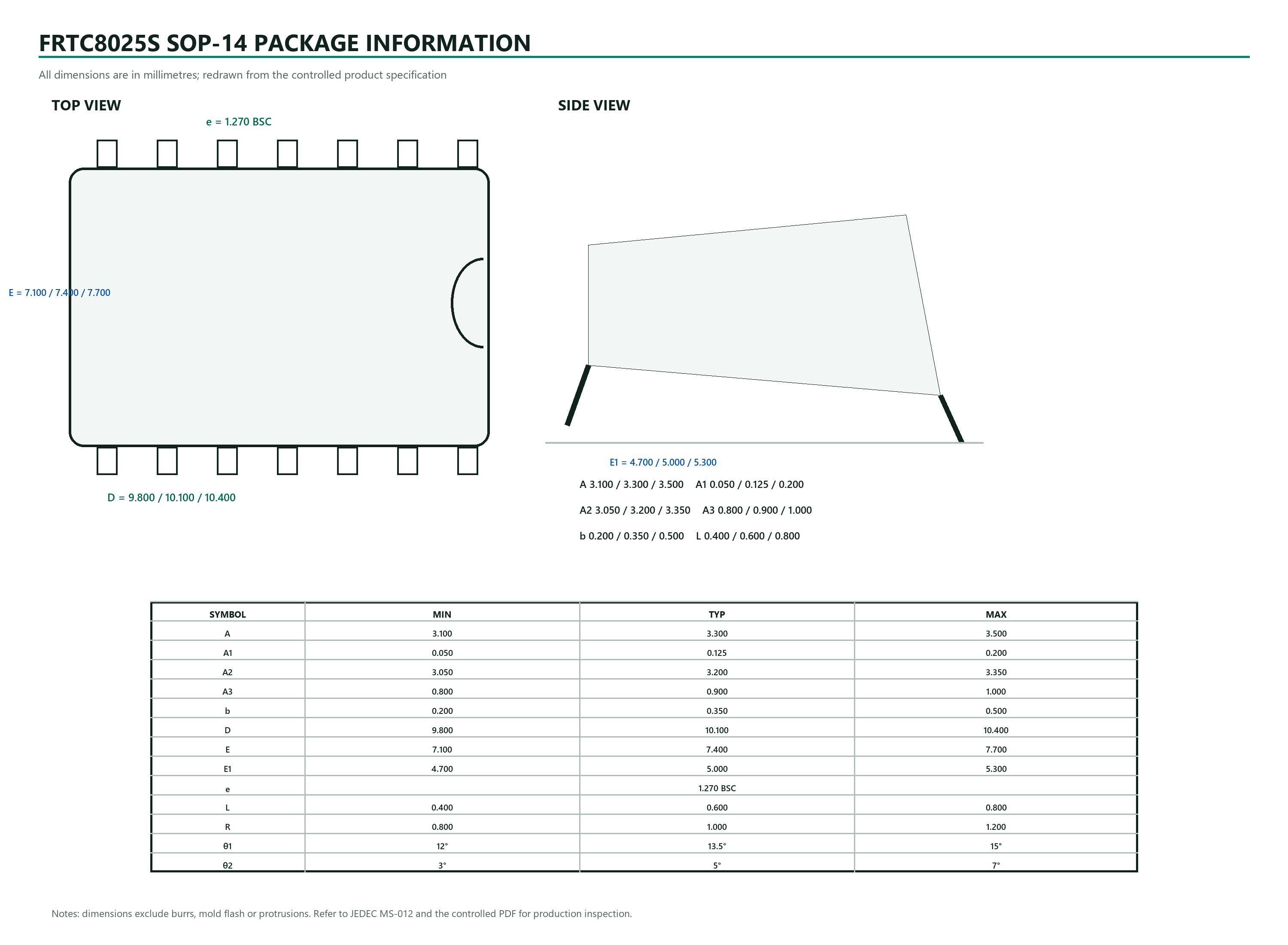
Package: SOP-14 with nominal body dimensions D = 10.100 mm and E = 7.400 mm, 1.270 mm lead pitch and 3.300 mm nominal overall height. The appearance image is not a dimensional drawing.
Application Guidance and Design Limitations
The PDF does not publish a target-application list. The following function-based evaluation contexts are derived from the integrated DTCXO, calendar, interrupt and compensated-output capabilities; they are not application approvals.
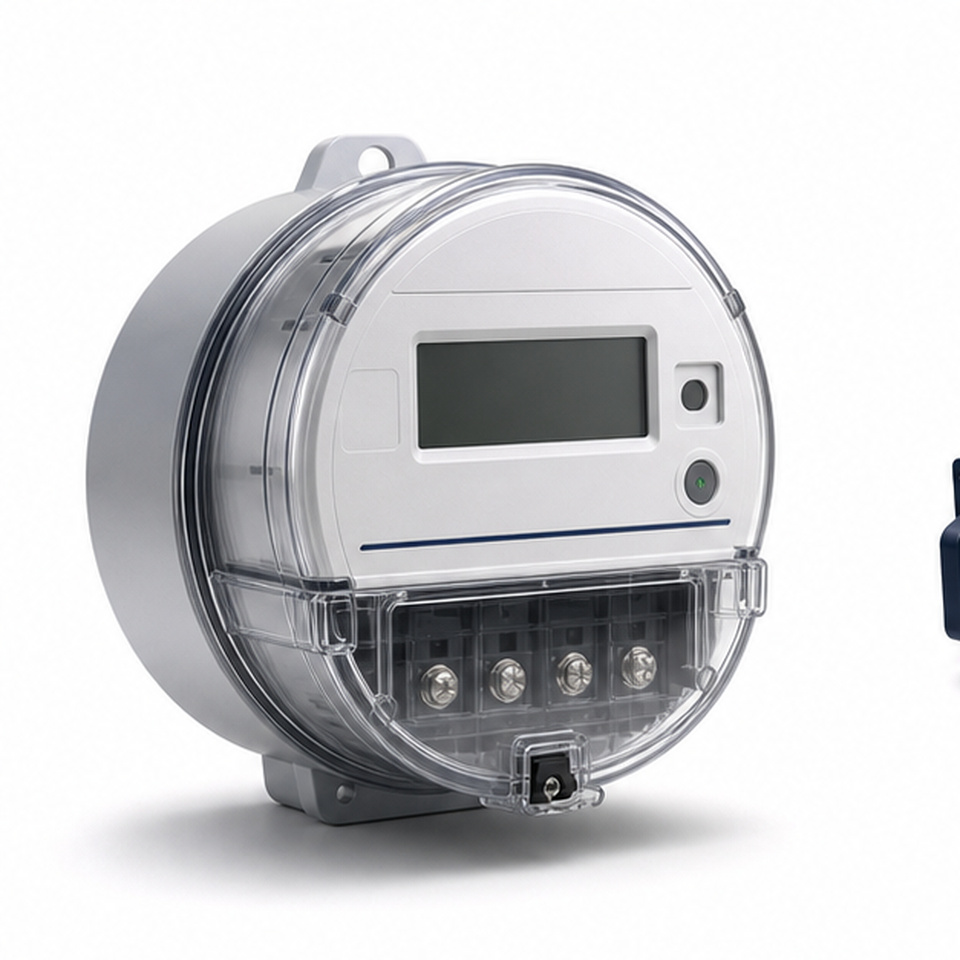 Electronic MeteringEvaluate stable local calendar time and scheduled records. Metrology, legal-time, security and audit requirements remain finished-system responsibilities.
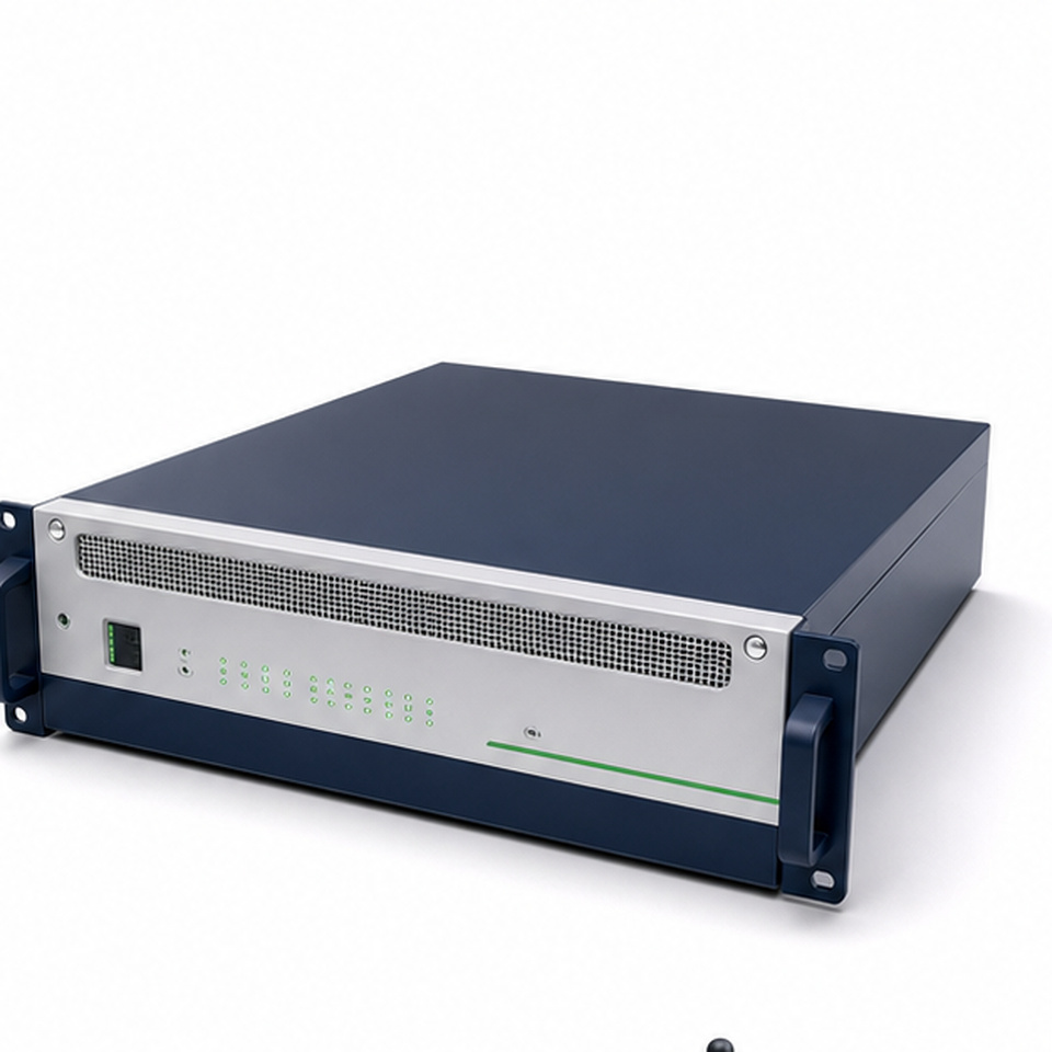 Telecom EquipmentUse the compensated RTC for local scheduling and maintenance timestamps. It is not a disciplined network-frequency reference.
 Industrial Data LoggingCombine calendar data, alarms and update events for local records. Validate rollover handling, time validity and external synchronization.
 Battery-Powered MonitoringUse timer or alarm events to schedule host activity. Verify total backup current and the voltage required for compensation and communication.
Application boundary: Validate accuracy, initialization, supply retention, I²C operation, interrupts, EMC, safety, assembly and environmental behavior in the complete product.
FRTC8025S Engineering FAQs
What is the FRTC8025S?
FRTC8025S is an I2C real-time clock module with an integrated 32.768 kHz temperature-compensated crystal oscillator, BCD calendar, three interrupt functions and a selectable compensated frequency output.
What frequency accuracy is specified for FRTC8025S?
At VDD = 3.0 V, the PDF lists ±1.5 ppm from 0 °C to +50 °C and ±3.0 ppm from -40 °C to +85 °C. These limits must not be separated from their stated voltage and temperature conditions.
What is the FRTC8025S I2C address?
The fixed 7-bit slave address is 0110010b, or 0x32. With the read/write bit appended, the 8-bit write address is 0x64 and the read address is 0x65.
Can FRTC8025S keep time below the normal interface voltage?
The recommended table lists VDD from 1.6 V to 5.5 V and a separate clock-retention voltage VCLK from 1.15 V to 5.5 V. Temperature compensation and host access require their applicable operating conditions; time retention alone does not imply full functionality.
Which interrupt functions does FRTC8025S provide?
It provides an alarm interrupt, a fixed-cycle timer interrupt and a selectable second- or minute-update interrupt. All share the open-drain /INT pin, so firmware should identify the source using AF, TF and UF.
Which FOUT frequencies are available?
FOUT can be selected as 32.768 kHz, 1024 Hz or 1 Hz. The output is temperature compensated and is enabled by FOE; when stopped, FOUT is high impedance.
How should firmware validate time after power-up?
Read VLF and VDET, initialize every required register when validity is uncertain, write valid BCD date and time data, and clear only the writable status flags as defined by the PDF.
Can FRTC8025S directly replace another SOP-14 RTC?
Not from package or interface alone. Compare pinout, 0x32 slave address, register map, DTCXO behavior, current, voltage-validity thresholds, interrupt handling, FOUT control and package dimensions before migration.
This page summarizes the FRTC8025S product specification for product evaluation and engineering reference. It does not replace the complete controlled specification. Confirm the current revision, register definitions, pin configuration, interface timing, absolute maximum ratings, validity thresholds, DTCXO behavior, package dimensions, PCB layout, assembly process and qualification requirements before production release.
Download FRTC8025S Product SpecificationContact NYFEA for Product Support