
FRTC8563 Wide-Temperature, Low-Current I²C Real-Time Clock
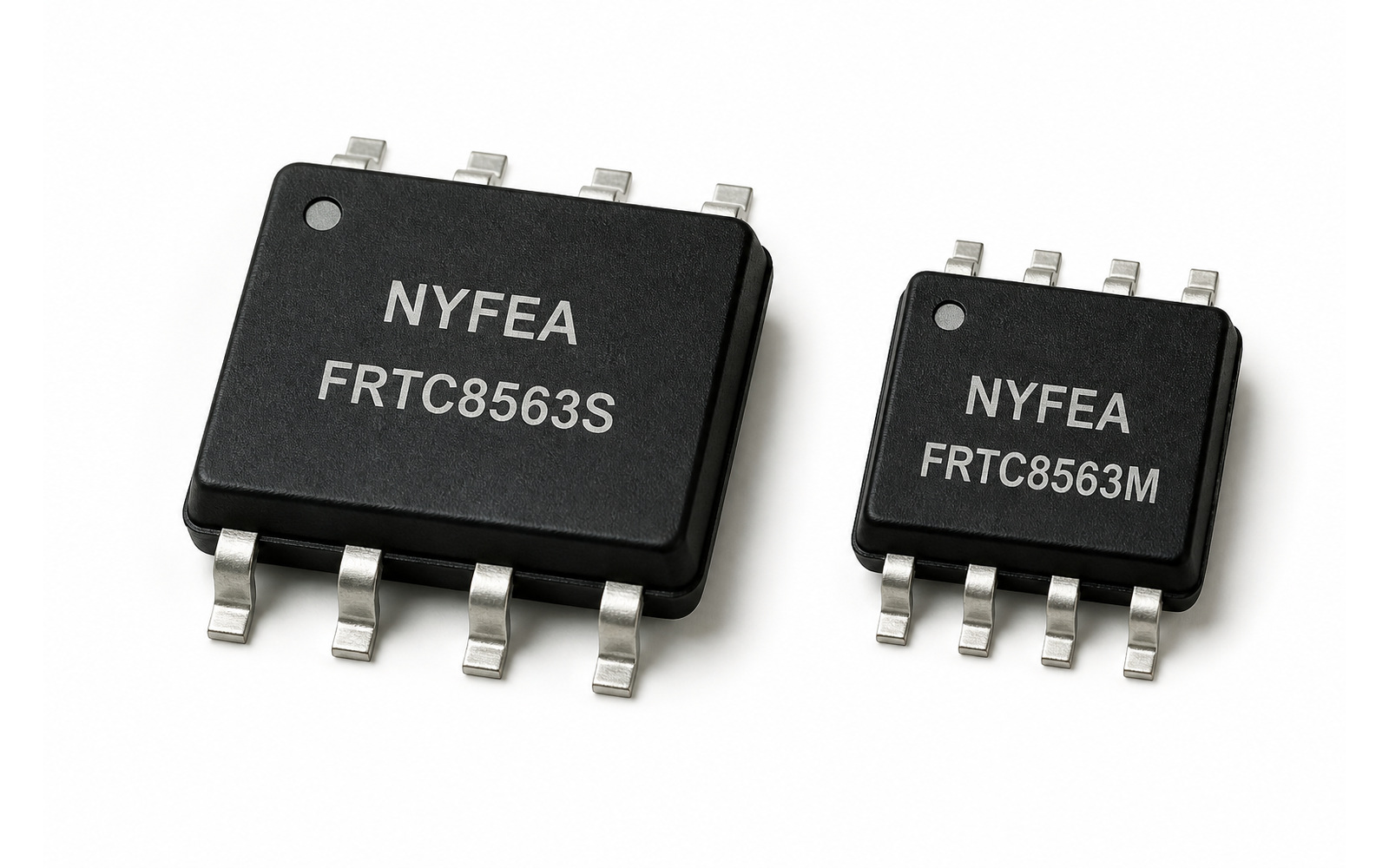
NYFEA FRTC8563 is a single-supply RTC with an external 32.768 kHz crystal, 24-hour BCD calendar, alarm interrupt, oscillator-stop flag and four-frequency square-wave output.
Product scope: FRTC8563 has no dedicated backup pin. Continued timekeeping requires the external power architecture to maintain VCC within the clock-data-integrity range. External-crystal accuracy, load capacitance and PCB parasitics remain system-level design responsibilities.
Use the current controlled PDF for register definitions, timing, test conditions, crystal design, package dimensions and production-release decisions.
Product Overview and Scope
FRTC8563 provides time and calendar data through a fixed-address I²C interface. It supports a 24-hour clock, automatic month-length adjustment, leap-year calculation within its two-digit year model, alarm comparison, oscillator-stop detection and programmable SQW output.
Selection boundary: The device is an RTC, not a temperature-compensated timebase. Calendar accuracy depends on the selected crystal, external load network, parasitic capacitance, temperature and PCB layout. Similar 8-pin RTCs are not automatically register-, address- or footprint-compatible.
Ordering Options and Key Features
| Part number | Package | Selection note |
|---|---|---|
| FRTC8563S | SOP-8 | Larger 1.27 mm lead pitch; use the SOP-8 controlled drawing. |
| FRTC8563M | MSOP-8 | Compact 0.65 mm lead pitch; use the MSOP-8 controlled drawing. |
24-Hour Calendar
BCD seconds, minutes, hours, weekday, date, month and two-digit year with leap-year handling.
Alarm Interrupt
Programmable comparison of minute, hour, date and weekday through the active-low open-drain /INT output.
Oscillator-Stop Flag
OSF reports uncertain clock integrity after an oscillator or relevant power event.
Programmable SQW
Open-drain output selectable to 32.768 kHz, 1.024 kHz, 32 Hz or 1 Hz.
Function Block and Pin Functions
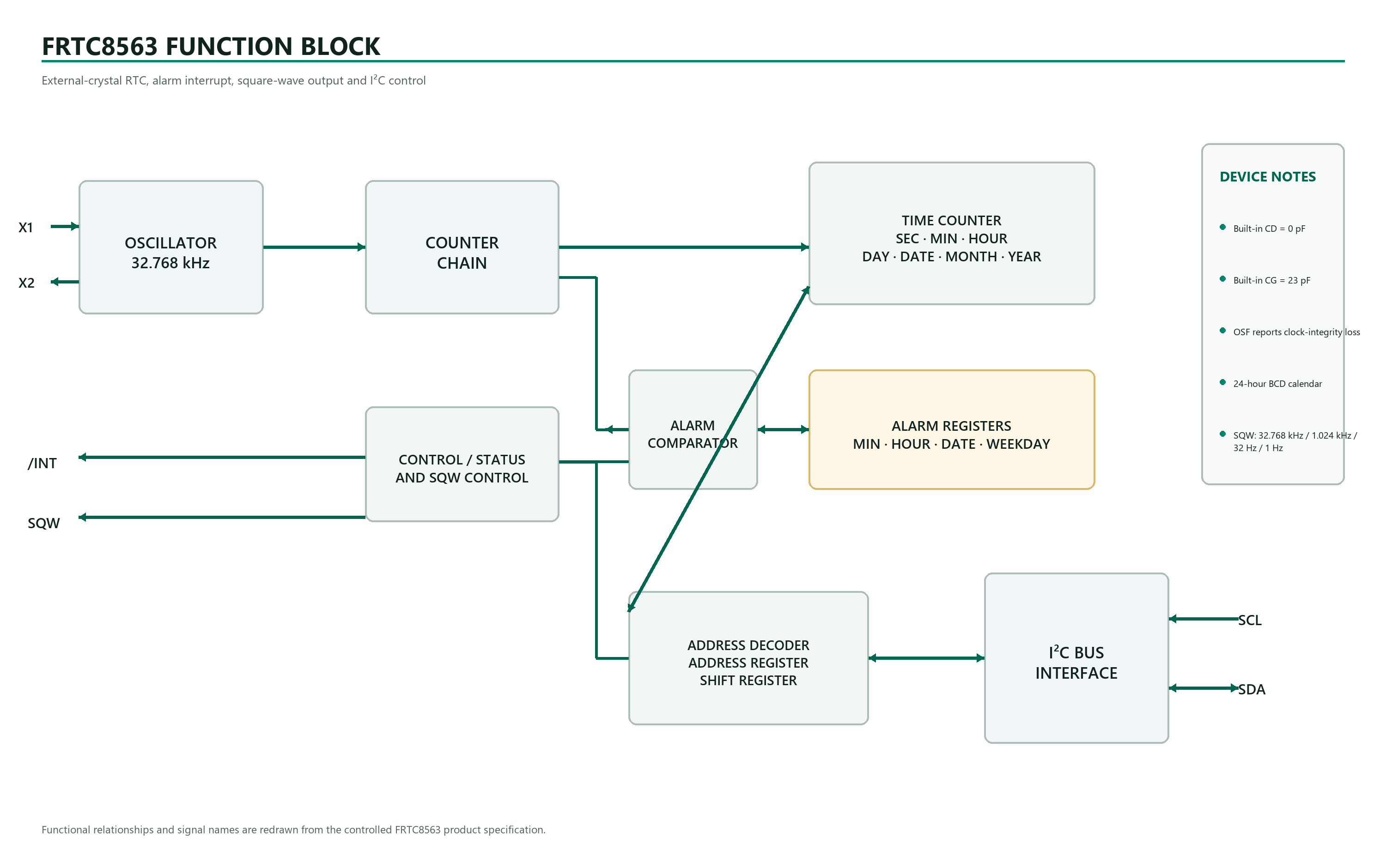
The external crystal drives the oscillator and counter chain. Calendar and alarm registers connect to the control, shift-register and I²C interface blocks, while /INT and SQW are managed by the control logic.
| Pin | Name | Function |
|---|---|---|
| 1 | X1 | 32.768 kHz oscillator input. |
| 2 | X2 | 32.768 kHz oscillator output. |
| 3 | /INT | Active-low open-drain alarm interrupt. |
| 4 | GND | Ground. |
| 5 | SDA | Open-drain I²C serial data; external pull-up required. |
| 6 | SCL | I²C serial clock input. |
| 7 | SQW | Open-drain programmable clock output. |
| 8 | VCC | Power supply. |
Calendar, Registers and Alarm
Calendar and alarm values use BCD. Firmware should validate legal ranges, read multi-byte time coherently and treat OSF as a time-validity warning.
| Address | Function | Engineering note |
|---|---|---|
| 0x00–0x01 | Control/status | Includes AF and AIE; preserve undefined or unimplemented bits as required. |
| 0x02–0x08 | Seconds through year | OSF is bit 7 of seconds; time uses 24-hour BCD format. |
| 0x09–0x0C | Alarm minute, hour, date, weekday | AE = 0 enables comparison for the corresponding field; AE = 1 ignores it. |
| 0x0D | SQW control | SQWE controls output enable; RS1:RS0 selects frequency. |
| Above 0x0D | No normal response | Test-mode addresses 0x49 and 0x4A must not be used. |
Alarm behavior: AF remains set until cleared by writing zero. After AF is cleared, it is set again only when the calendar advances into another enabled match condition.
I²C Interface, Read Mode and Write Mode
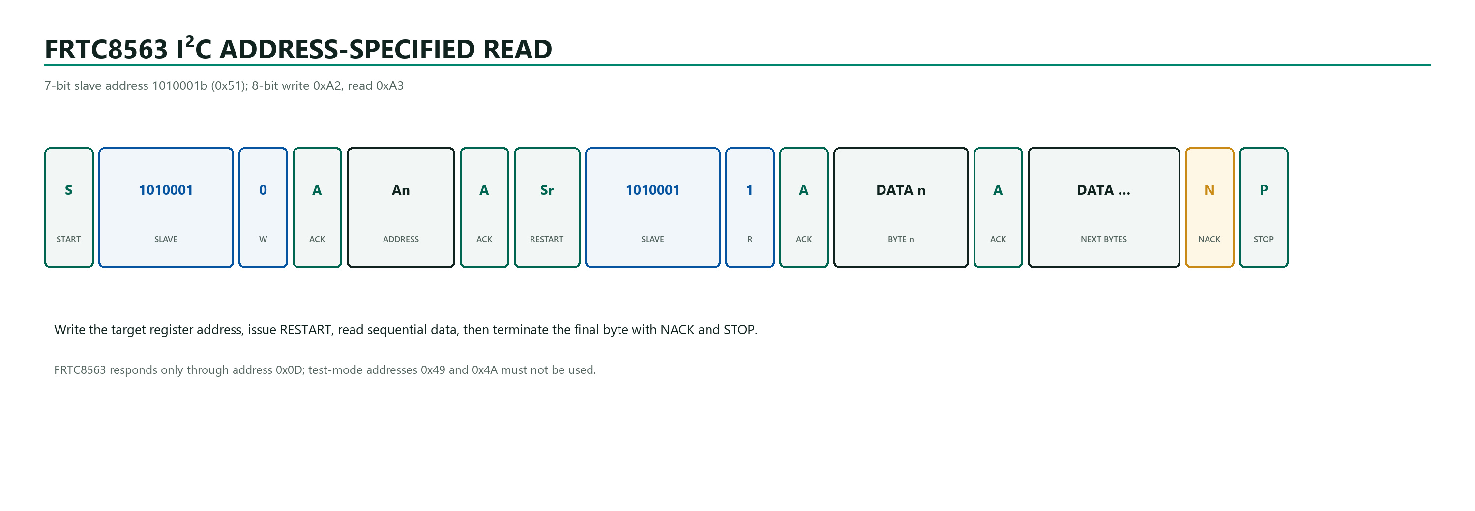
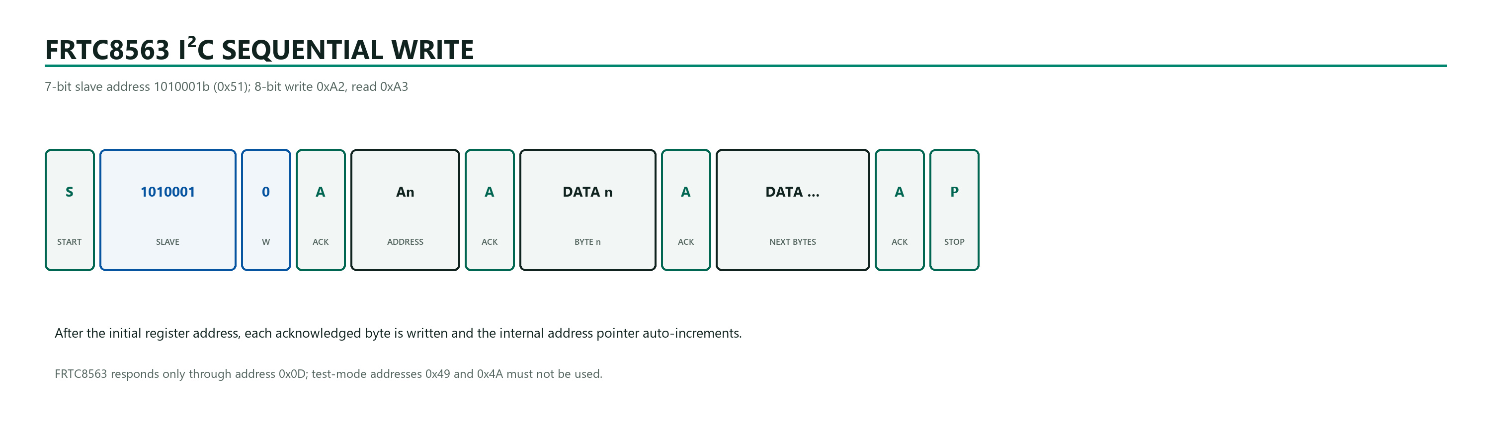
| 7-bit slave address | 1010001b = 0x51 |
|---|---|
| 8-bit transfer address | 0xA2 for write; 0xA3 for read |
| Bus speed | Up to 400 kHz; Fast-mode timing is specified |
| Data output | SDA is open-drain; use bus pull-ups sized for the rail and capacitance |
| Auto-increment | The internal address advances during sequential read and write transfers |
Power, Current and Time Validity
| Active interface supply | VCC = 1.7 V to 5.5 V |
|---|---|
| Clock-data integrity | VCC = 1.5 V to 5.5 V with the interface inactive; this is not the full-interface range |
| Reliable oscillator startup | At power-up, the PDF requires VCC(min)power-up = applicable VCC(min) + 0.3 V |
| 3 V, interface inactive, SQW disabled | 400 nA typical, 800 nA maximum; feature-summary typical value is stated at 25 °C |
| 5 V, interface inactive, SQW disabled | 450 nA typical, 900 nA maximum |
| 3 V, SQW enabled at 32 kHz | 600 nA typical, 850 nA maximum with the interface inactive |
| No dedicated backup pin | The system must maintain VCC using an external source-selection or hold-up circuit |
Estimate retention life using maximum device current, regulator and switch leakage, pull-up paths, source self-discharge, temperature and the minimum voltage required by the intended operating state.
Electrical and Clock Characteristics
| Operating ambient temperature | -40 °C to +125 °C |
|---|---|
| Absolute-maximum storage | -65 °C to +150 °C; stress rating only, not an operating condition |
| Interface-active current | 15 µA maximum at 100 kHz or 25 µA maximum at 400 kHz |
| I²C bus capacitance | 400 pF maximum per bus line under the AC timing table |
| Crystal frequency | 32.768 kHz nominal |
| Crystal ESR | 70 kΩ maximum |
| Crystal load capacitance | 6 pF or 12.5 pF |
| SQW output | Open-drain; 32.768 kHz, 1.024 kHz, 32 Hz or 1 Hz |
Accuracy boundary: The PDF specifies the crystal requirements and load-capacitor guidance but does not publish a complete guaranteed RTC time-accuracy value. Finished accuracy requires crystal tolerance, temperature behavior, aging and PCB parasitics to be included.
Typical Application and Recommended Crystal Layout
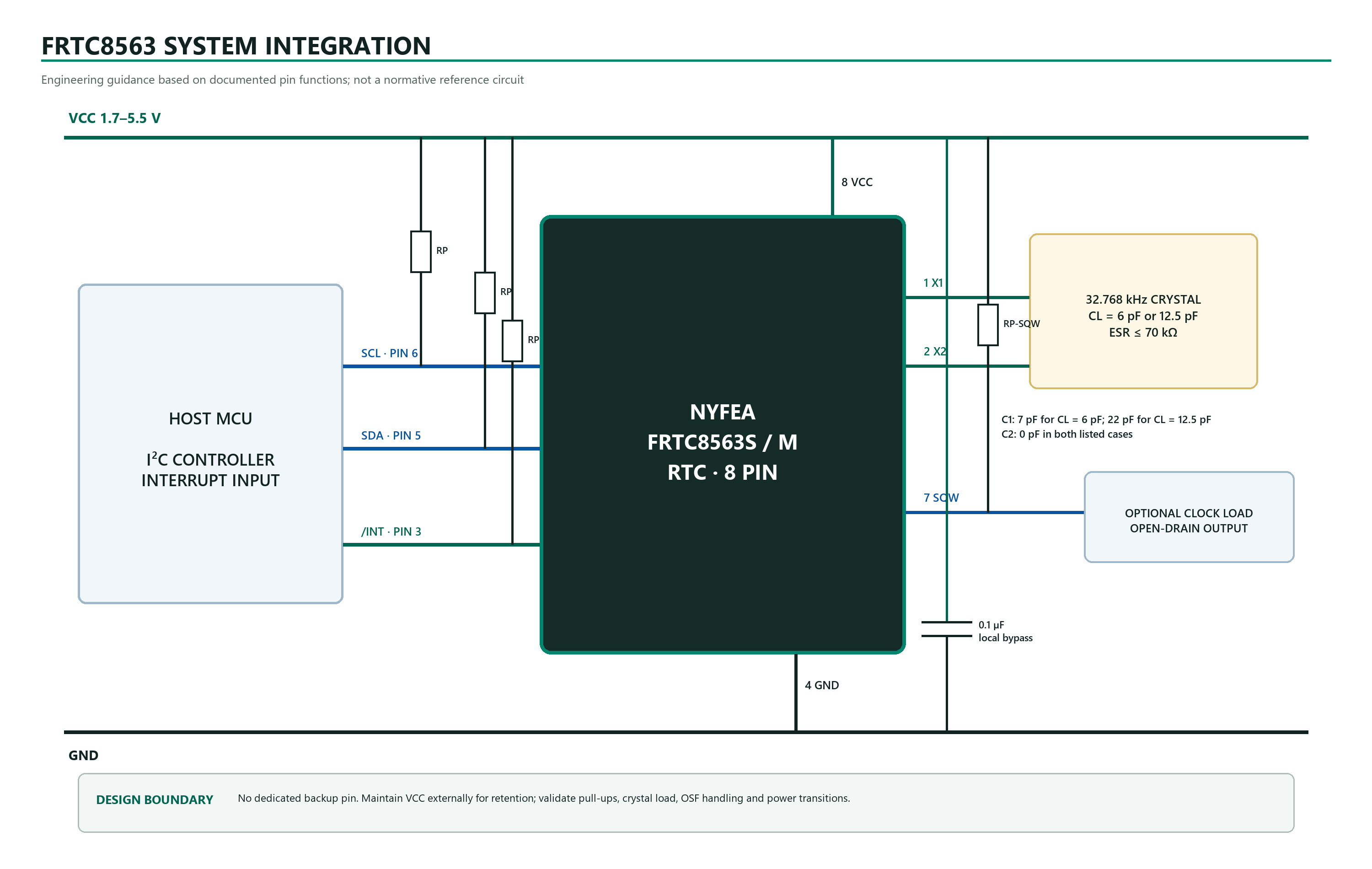
The controlled PDF does not label a normative typical application circuit. The first drawing organizes the documented supply, crystal, I²C, /INT and SQW connections; the second redraws the recommended guarded crystal layout.
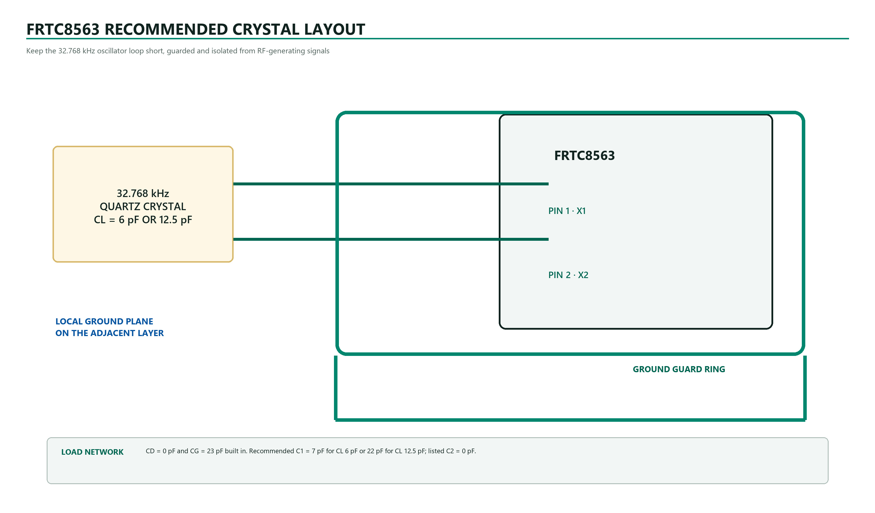
- The PDF lists built-in CD = 0 pF and CG = 23 pF.
- For CL = 6 pF, the listed recommendation is C1 = 7 pF and C2 = 0 pF; for CL = 12.5 pF, C1 = 22 pF and C2 = 0 pF.
- Include all X1-to-X2 parasitic capacitance in the load calculation.
- SDA, /INT and SQW are open-drain outputs and require suitable pull-ups when used.
Package Information
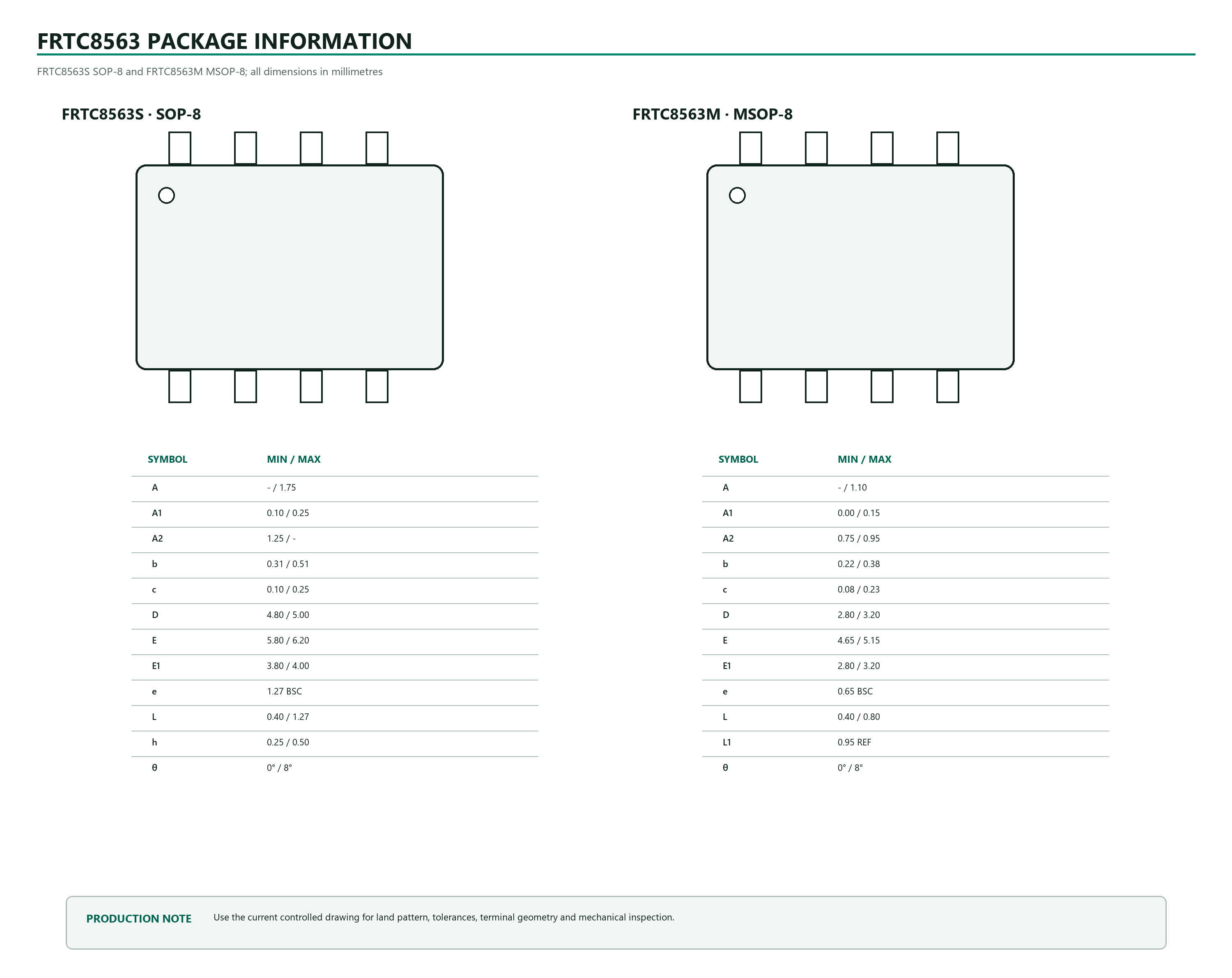
FRTC8563 is offered as FRTC8563S in SOP-8 and FRTC8563M in MSOP-8. The packages have the same functional pin numbering but different body dimensions and lead pitch.
Application Guidance and Design Limitations
The controlled specification explicitly lists the six application groups below. These examples describe evaluation contexts, not finished-product approval or certification.
 Digital Still CamerasUse calendar time for photo timestamps and scheduled functions. Validate oscillator accuracy, OSF handling and supply retention.
 Digital Video CamerasApply the RTC to recording timestamps and local schedules. Verify crystal behavior across enclosure temperature and power events.
 PrintersSupport job records and scheduled maintenance while validating I²C integrity and immunity to motor and power noise.
 Copy MachinesUse local calendar, alarm and SQW functions only after validating supply hold-up and service-event time recovery.
 Mobile EquipmentEvaluate low-current time retention for portable terminals. Source selection, backup life and valid-time recovery remain external.
 Battery-Powered DevicesMaintain VCC within the required range and verify the complete backup-current and leakage budget.
Application boundary: Validate crystal accuracy, initialization, time validity, supply transitions, I²C operation, open-drain outputs, EMC, safety, assembly and environmental behavior in the complete product.
FRTC8563 Engineering FAQs
What is the FRTC8563?
FRTC8563 is a two-wire I²C real-time clock that uses an external 32.768 kHz crystal. It provides a 24-hour BCD calendar, one alarm, an oscillator-stop flag and a selectable open-drain square-wave output.
What is the FRTC8563 I²C address?
The fixed 7-bit slave address is 1010001b, or 0x51. With the read/write bit appended, the 8-bit write address is 0xA2 and the read address is 0xA3.
What supply voltage does FRTC8563 require?
The recommended active-interface supply is 1.7 V to 5.5 V. The DC table separately lists 1.5 V to 5.5 V for clock-data integrity with the interface inactive. Retention voltage must not be presented as full-interface operation.
How much current does FRTC8563 consume?
The feature summary lists 400 nA typical at VCC = 3.0 V and TA = 25 °C. In the DC table, the interface-inactive, SQW-disabled condition at 3.0 V is 400 nA typical and 800 nA maximum; include the output and interface conditions when quoting current.
Which square-wave frequencies are available?
SQW can output 32.768 kHz, 1.024 kHz, 32 Hz or 1 Hz when SQWE is enabled. SQW is open-drain and therefore requires an appropriate pull-up and load design.
How should the 32.768 kHz crystal be selected?
The specification lists 6 pF or 12.5 pF load capacitance and 70 kΩ maximum ESR. It also lists C1 = 7 pF for a 6 pF crystal or 22 pF for a 12.5 pF crystal, with C2 = 0 pF in both cases; parasitic capacitance must be included in the final calculation.
What does the OSF flag mean?
OSF = 1 indicates that clock integrity is no longer guaranteed. Firmware should reinitialize and set valid time and date data after a power or oscillator event instead of accepting the retained calendar blindly.
Are FRTC8563S and FRTC8563M mechanically interchangeable?
They share the same functional pin numbering but use different packages: FRTC8563S is SOP-8 and FRTC8563M is MSOP-8. PCB footprints and mechanical dimensions are not interchangeable.
This page summarizes the FRTC8563 product specification for product evaluation and engineering reference. It does not replace the complete controlled specification. Confirm the current revision, register definitions, pin configuration, interface timing, electrical limits, crystal network, package dimensions, PCB layout, assembly process and qualification requirements before production release.
Download FRTC8563 Product SpecificationContact NYFEA for Product Support