
FRTC8900 High-Stability DTCXO I²C Real-Time Clock
NYFEA FRTC8900 integrates a 32.768 kHz DTCXO, BCD calendar, alarm, wake-up timer, time-update interrupt, compensated FOUT and automatic VDD/VBAT switchover.
Product scope: FRTC8900 manages RTC supply switchover and provides a configurable charge path, but it is not a complete battery charger or safety controller. Backup-source chemistry, protection, charge limits, time validity and system power sequencing remain design responsibilities.
Use the current controlled PDF for register definitions, timing, package dimensions and production-release decisions.
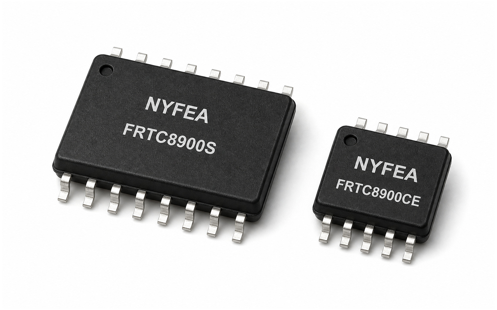
Product Overview and Scope
FRTC8900 is an I²C RTC module with an integrated temperature-compensated 32.768 kHz oscillator. It retains a calendar from year through second, provides programmable interrupt functions, exposes compensated FOUT under FOE control and manages normal/backup supply paths.
Selection boundary: Similar I²C functionality does not establish drop-in compatibility. Verify the 0x32 address, register banks, package pinout, VDD/VBAT architecture, interrupt behavior and initialization sequence before migration.
Ordering Options and Key Features
| Ordering code | Package | Frequency-stability condition | Specified limit |
|---|---|---|---|
| FRTC8900S | SOP-14, 10.1 mm × 7.1 mm class | TA = 0 °C to +50 °C, VDD = 3.0 V | ±1.5 ppm |
| FRTC8900S | SOP-14 | TA = -40 °C to +85 °C, VDD = 3.0 V | ±3 ppm |
| FRTC8900CE | 3225-10, 3.2 mm × 2.5 mm | TA = -40 °C to +85 °C, VDD = 3.0 V | ±3 ppm |
Compensated timebase
Integrated DTCXO and temperature sensor support compensated calendar time and FOUT.
Calendar and events
Leap-year calendar from 2000 to 2099, alarm, fixed-cycle timer and time-update interrupt.
Backup management
VDD/VBAT switchover, detection flags and configurable backup-control registers.
Low-current operation
0.54 µA typical at 3 V under the stated FOUT-off, interface-idle and detection conditions.
Function Block and Pin Functions
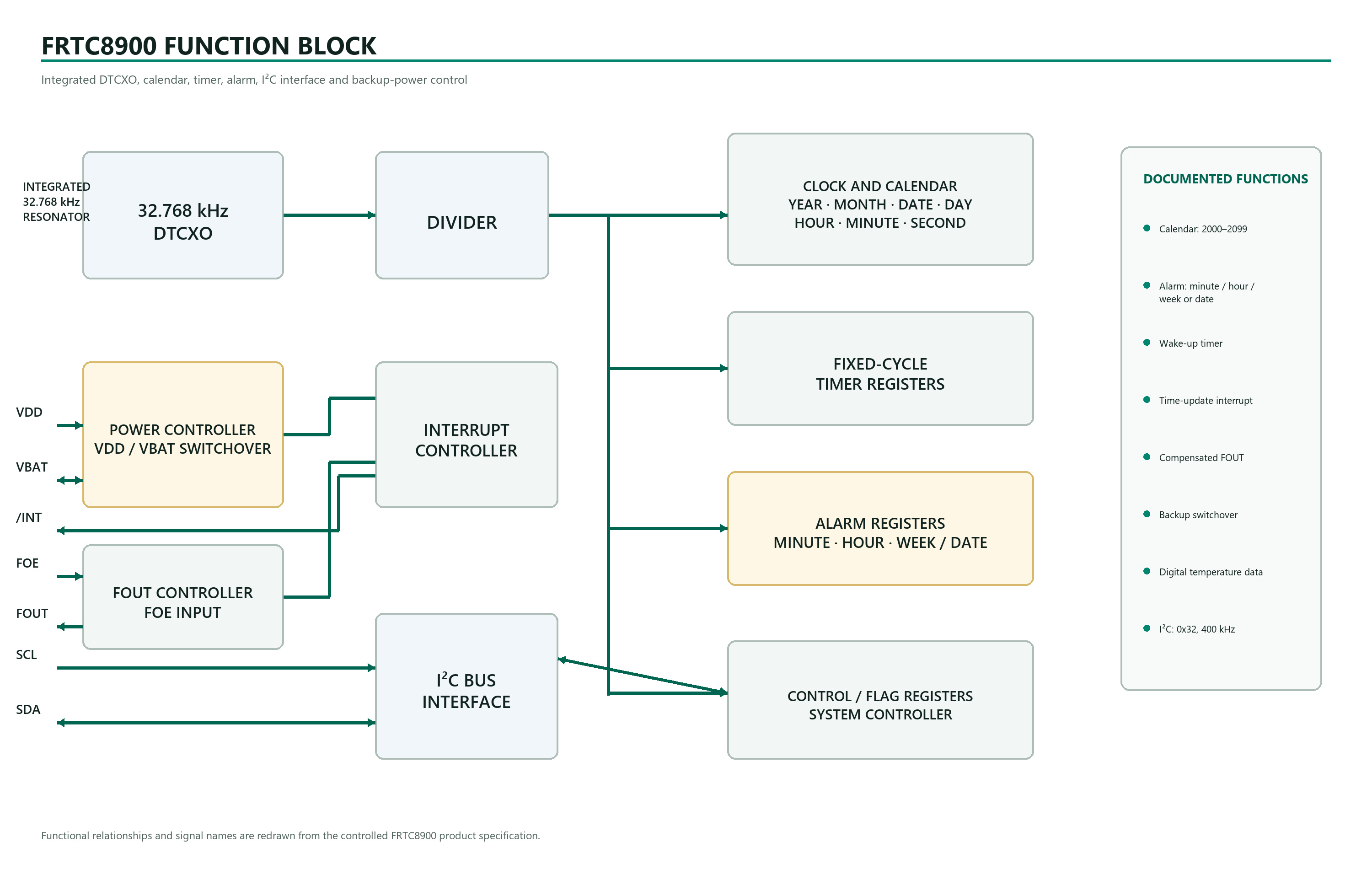
| Signal | 3225-10 pin | SOP-14 pin | Function |
|---|---|---|---|
| FOE | 1 | 7 | Controls FOUT enable; input. |
| VDD | 2 | 6 | Normal-mode positive supply. |
| VBAT | 3 | 5 | Backup supply; connect to VDD when backup switching is not used. |
| FOUT | 4 | 3 | CMOS frequency output controlled by FOE and FSEL. |
| SCL | 5 | 2 | I²C serial-clock input. |
| T1 / T2 | 6 / 8 | 1 / 12 | Manufacturer test pins; do not connect externally. |
| SDA | 7 | 13 | I²C open-drain serial data input/output; requires a pull-up. |
| GND | 9 | 11 | Ground. |
| /INT | 10 | 10 | Open-drain alarm, timer and time-update interrupt output. |
| N.C. | — | 4, 8, 9, 14 | Not internally connected; follow the controlled specification. |
Timekeeping, Registers and Interrupts
Calendar data are BCD encoded. The basic and extension register banks include time, calendar, alarm, timer, flag, control, temperature-data and backup-control fields.
| Function | Engineering interpretation |
|---|---|
| Calendar | Year, month, date, weekday, hour, minute and second; automatic leap-year correction from 2000 to 2099. |
| Alarm | Minute, hour and either weekday or date are compared according to WADA and AE-bit settings. |
| Fixed-cycle timer | Periodic event range stated as 244.14 µs to 4095 minutes; TF records the event and TIE controls /INT. |
| Time-update interrupt | Selectable second or minute update event; UF records the event and UIE controls /INT. |
| Validity flags | VLF reports compromised clock data; VDET reports loss of reliable temperature compensation. |
| Temperature data | Digital temperature data are updated during compensation activity; conversion follows the PDF equation. |
Initialization rule: After initial power-up or whenever VLF = 1, initialize all registers before using the calendar. The specification states that read access is possible after 30 ms, while stable time/calendar setup requires the oscillator-start interval.
I²C Interface, Read Mode and Write Mode
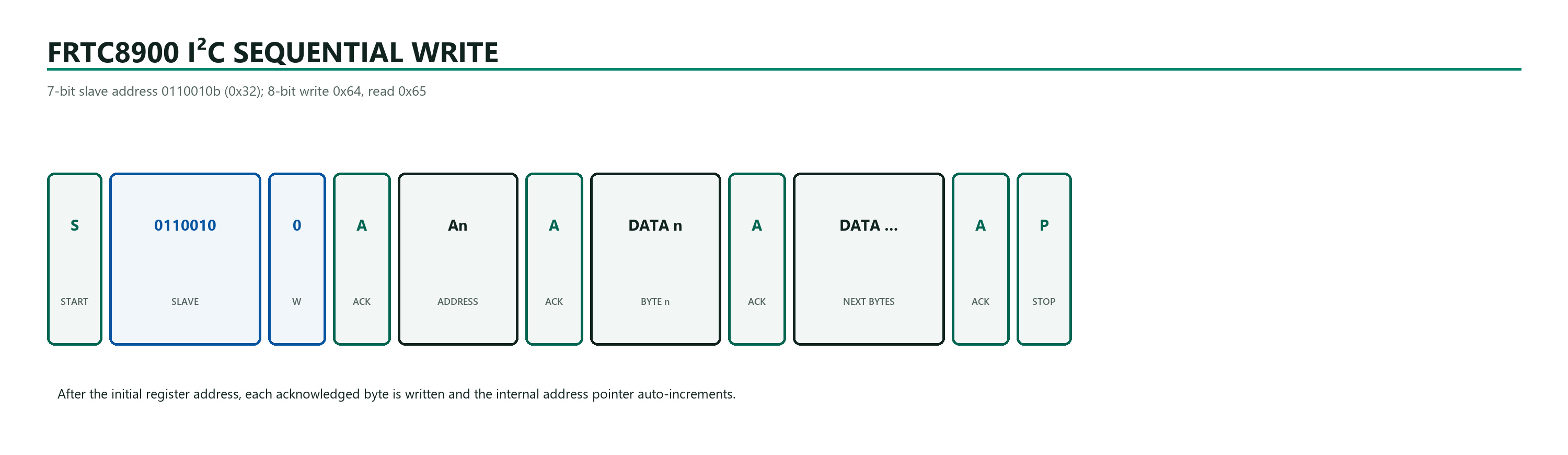
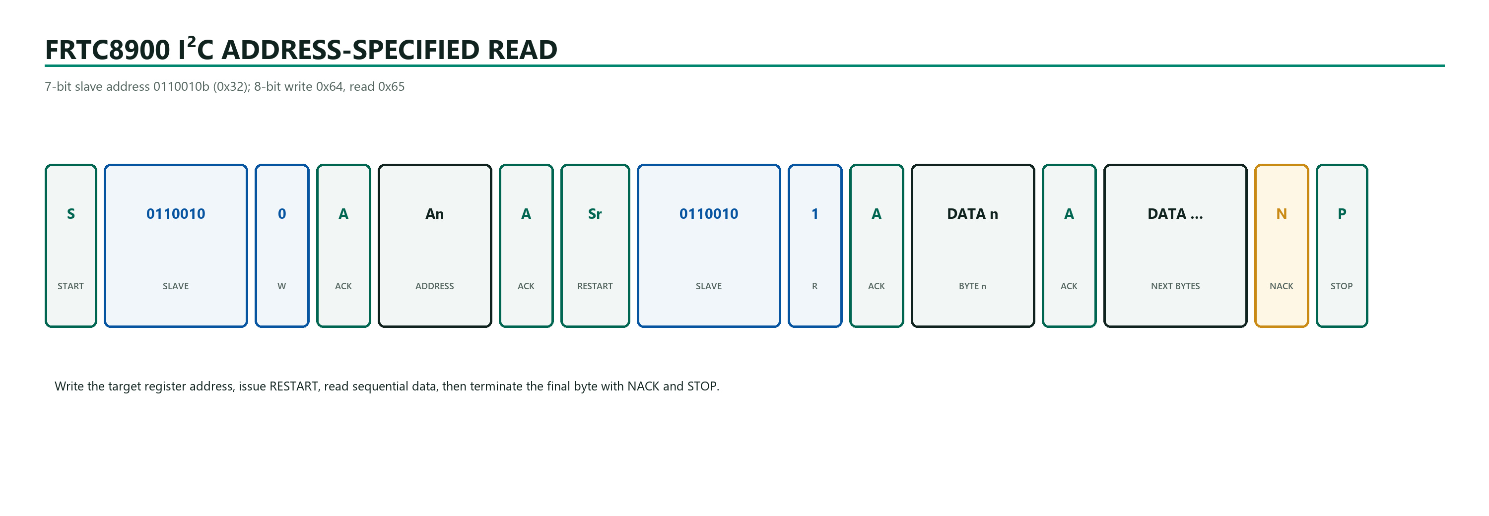
| 7-bit slave address | 0110010b = 0x32 |
|---|---|
| 8-bit address bytes | Write 0x64; read 0x65 |
| Bus modes | Standard mode and fast mode, up to 400 kHz |
| Data line | SDA is open-drain and requires a suitable pull-up for bus capacitance and timing. |
| Address pointer | Automatically increments after each transferred byte; basic and extension banks have documented wrap sequences. |
Power, Backup, Trickle Charge and Time Validity
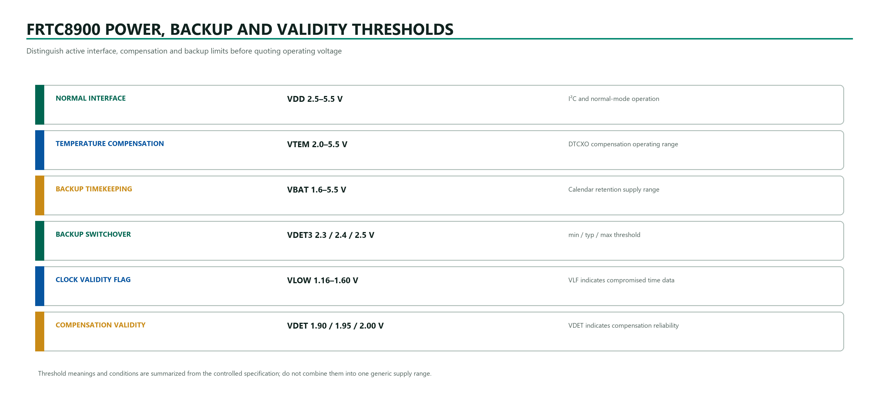
| Parameter | Minimum | Typical | Maximum |
|---|---|---|---|
| Normal-mode VDD | 2.5 V | 3.0 V | 5.5 V |
| Backup VBAT | 1.6 V | 3.0 V | 5.5 V |
| Temperature-compensation voltage | 2.0 V | 3.0 V | 5.5 V |
| Backup switchover VDET3 | 2.3 V | 2.4 V | 2.5 V |
| Compensation-validity VDET | 1.90 V | 1.95 V | 2.00 V |
| Clock-validity VLOW | 1.16 V | — | 1.60 V |
The backup-control register controls VDD detection and internal switch operation. Detection occurs periodically, and the BKSMP setting trades detection duration, current consumption, transition behavior and charge-path effectiveness. Validate fast VDD falls, noise, leakage and recovery in the assembled system.
Electrical and Frequency Characteristics
| Parameter | Condition | Typical | Maximum / limit |
|---|---|---|---|
| FOUT-off current at 3 V | fSCL = 0, /INT high, FOE low, VDD = VBAT, 2 s compensation interval, 2 ms detection period | 0.54 µA | 2.2 µA |
| FOUT-off current at 5 V | Same stated condition | 0.59 µA | 2.4 µA |
| FOUT-on current at 3 V | FOE high, 32.768 kHz, CL = 0 pF; remaining stated condition | 1.18 µA | 2.8 µA |
| FOUT-on current at 5 V | Same stated condition | 1.66 µA | 3.4 µA |
| Frequency / voltage characteristic | TA = +25 °C, VDD = 2.0 V to 5.5 V | — | ±1 ppm |
| Oscillator start | -40 °C to +85 °C, VDD = 1.6 V to 5.5 V | — | 1 s |
| First-year aging | TA = +25 °C, VDD = 3.0 V | — | ±3 ppm |
| Temperature-sensor accuracy | VDD = 3.0 V | — | ±4 °C |
| FOUT duty | 50% of VDD level | 50% | 40% to 60% |
Absolute maximum is not operating guidance: The PDF separately lists -55 °C to +125 °C storage and -0.3 V to 6.5 V supply stress ratings. Use the recommended operating table for functional design.
Typical Application Circuit
The PDF example shows VDD and VBAT decoupling, FOE/FOUT, I²C pull-ups, /INT and a backup-source path. It is a connection reference, not a complete battery-management design.
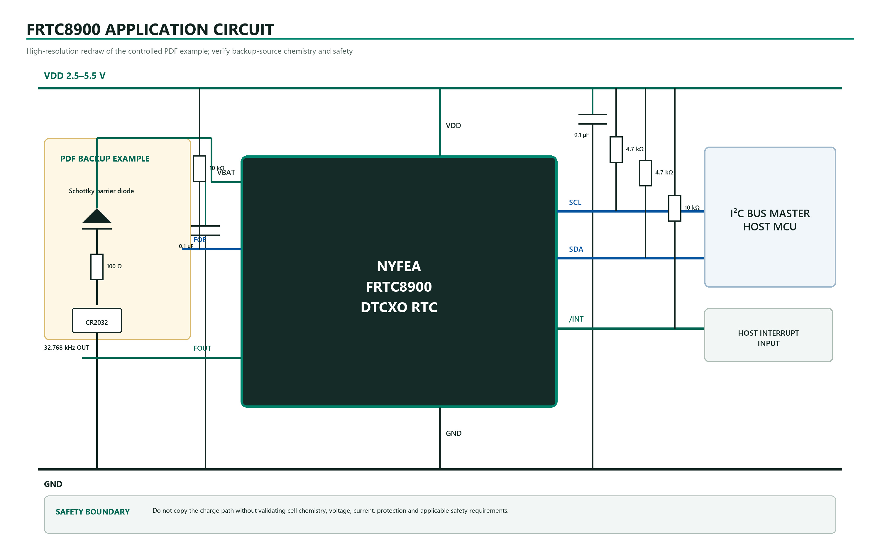
Backup-source safety: The drawing reproduces the PDF-labelled example, but a product designer must independently confirm whether the chosen cell or capacitor may be charged. Do not apply a charge path to a non-rechargeable source.
Package Information
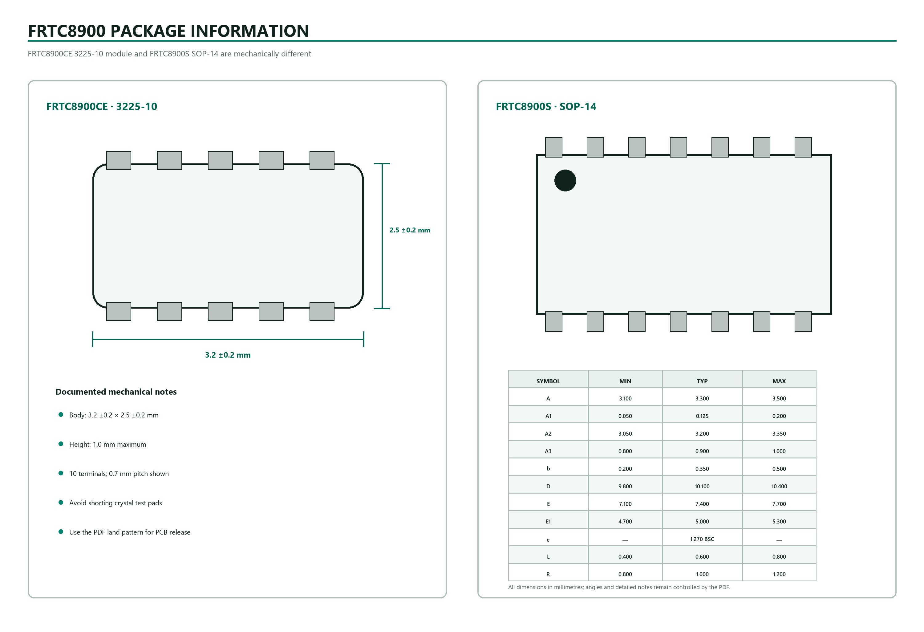
FRTC8900CE and FRTC8900S use different mechanical formats and footprints even though their functional signal sets correspond.
Application Guidance and Design Limitations
The controlled specification does not publish an approved target-application list. The six function-based evaluation contexts below illustrate where stable local time, backup retention, alarms or event timestamps may be useful; they are not application certifications.
 Precision Data LoggingEvaluate compensated timestamps, backup retention and VLF/VDET recovery for chronological sensor records.
 Smart Metering EvaluationUse calendar and event functions only after validating legal-time, accuracy, retention and qualification requirements.
 Network Appliance Event LogsProvide stable local event time; FRTC8900 is not automatically a network-disciplined or traceable time source.
 Access-Control Event RecordsEvaluate retained timestamps and scheduled events while protecting personal data and validating complete-system security.
 Portable Field InstrumentsBudget normal and backup current, leakage and recovery before relying on long-term unattended timekeeping.
 Industrial SchedulingUse alarm, timer and update interrupts after validating EMC, power events, initialization and host fault handling.
Application boundary: Validate accuracy, initialization, time validity, backup life, charging safety, I²C operation, interrupts, EMC, assembly and environmental behavior in the complete product.
FRTC8900 Engineering FAQs
What is the FRTC8900?
FRTC8900 is an I²C real-time clock with an integrated 32.768 kHz temperature-compensated crystal oscillator. It combines BCD calendar timekeeping, alarm, fixed-cycle timer, time-update interrupt, compensated FOUT, digital temperature data and backup-source management.
What is the FRTC8900 I²C address?
The fixed 7-bit slave address is 0110010b, or 0x32. With the read/write bit appended, the 8-bit write byte is 0x64 and the read byte is 0x65.
What frequency stability is specified?
FRTC8900S is specified at ±1.5 ppm from 0 °C to +50 °C and ±3 ppm from -40 °C to +85 °C at VDD = 3.0 V. FRTC8900CE is specified at ±3 ppm from -40 °C to +85 °C at VDD = 3.0 V. Preserve the suffix, temperature and supply conditions when quoting accuracy.
What are the FRTC8900 supply ranges?
Normal-mode VDD is 2.5 V to 5.5 V. The backup-supply range is 1.6 V to 5.5 V, while the temperature-compensation range is 2.0 V to 5.5 V. These conditions are not interchangeable and should not be collapsed into one generic operating-voltage statement.
How much current does FRTC8900 consume?
With fSCL = 0 Hz, /INT high, FOE low, FOUT disabled, VDD = VBAT, a 2 s compensation interval and a 2 ms VDET3 measurement period, the table lists 0.54 µA typical and 2.2 µA maximum at 3 V. FOUT-enabled current is specified separately.
Can the trickle-charge circuit be used with any battery?
No. The RTC is not a complete charger or battery-safety controller. Validate the storage chemistry, maximum charging voltage and current, reverse-current path, temperature limits and required protection before enabling any charging path.
What timer range is documented?
The fixed-cycle timer can generate periodic events over a range stated as 244.14 µs to 4095 minutes. Firmware must configure the source and preset correctly and handle TF and /INT according to the register description.
Are FRTC8900S and FRTC8900CE mechanically interchangeable?
No. FRTC8900S is a 10.1 mm × 7.1 mm class SOP-14 package, while FRTC8900CE is a 3.2 mm × 2.5 mm 10-terminal module. Their footprints, dimensions and pin positions are different.
Technical source and design authority
This page summarizes the FRTC8900 product specification for product evaluation and engineering reference. It does not replace the complete controlled specification. Confirm the current revision, register definitions, pin configuration, interface timing, electrical limits, backup-source design, package dimensions, PCB layout, assembly process and qualification requirements before production release.
Download FRTC8900 Product SpecificationContact NYFEA for Product Support