
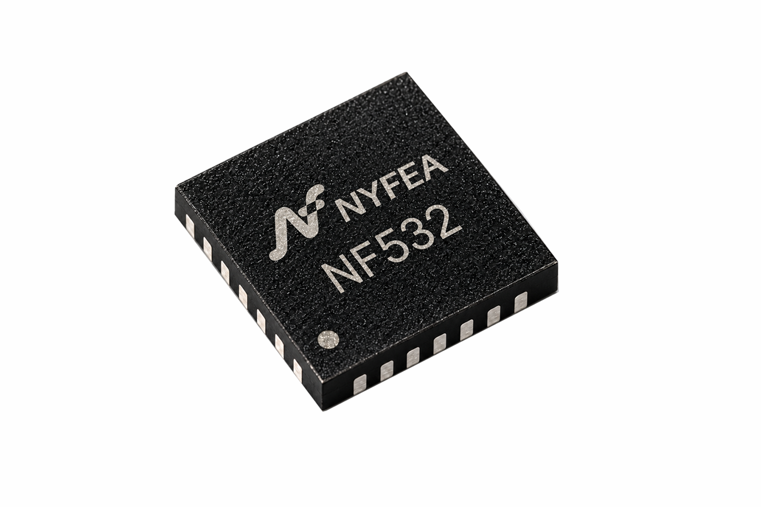
Product Overview and Selection Scope
NF532 integrates the digital protocol engine, an 80C51-compatible microcontroller core, on-chip memory, a 13.56 MHz RF interface and host connectivity. The device can operate as a reader/writer, emulate selected card technologies or establish an ISO/IEC 18092 peer-to-peer link.
The supplied NF532 document identifies engineering-draft package and ordering information. Confirm the current orderable code, package qualification and production status before procurement or PCB release.
Contactless Operating Modes
The six documented operating modes support common reader, target and peer-to-peer system architectures.
Architecture and Host Interfaces
| Function | Documented capability | Engineering use |
|---|---|---|
| Controller and memory | 80C51 core, 40 KB ROM, 1 KB RAM | Embedded protocol and application control. |
| Host interfaces | SPI, I²C and high-speed UART | Connection to the host processor or application controller. |
| Host I/O supply | PVDD: 1.6 V to 3.6 V | Defines the digital host-interface voltage domain. |
| Clock | 27.12 MHz crystal oscillator | Reference clock for RF and digital operation. |
| Power management | Integrated LDO, secure-IC supply switch and power-down modes | Supports compact, energy-managed contactless systems. |
Verified Electrical Characteristics
| Parameter | Documented value | Engineering note |
|---|---|---|
| Main supply (VBAT) | 2.7 V to 5.5 V | Follow the supply and decoupling requirements in the current specification. |
| Host-interface supply (PVDD) | 1.6 V to 3.6 V | Sets the host digital I/O voltage domain. |
| Ambient temperature | −30 °C to +85 °C | Operating ambient range in the quick-reference data. |
| Hard power-down current | 2 µA maximum at 5 V | IC condition only; other board loads are excluded. |
| Software power-down current | 45 µA maximum at 5 V with RF level detector enabled | Verify the documented firmware state and test conditions. |
| Typical reader/P2P range | Up to 50 mm | Conditional typical result, not a guaranteed system limit. |
| Typical card-emulation range | Approximately 100 mm | Depends on the initiator, antenna system and test setup. |
Antenna geometry, Q factor, tuning, supply, target device, orientation, enclosure and nearby materials determine the final operating distance.
Typical Application Circuit
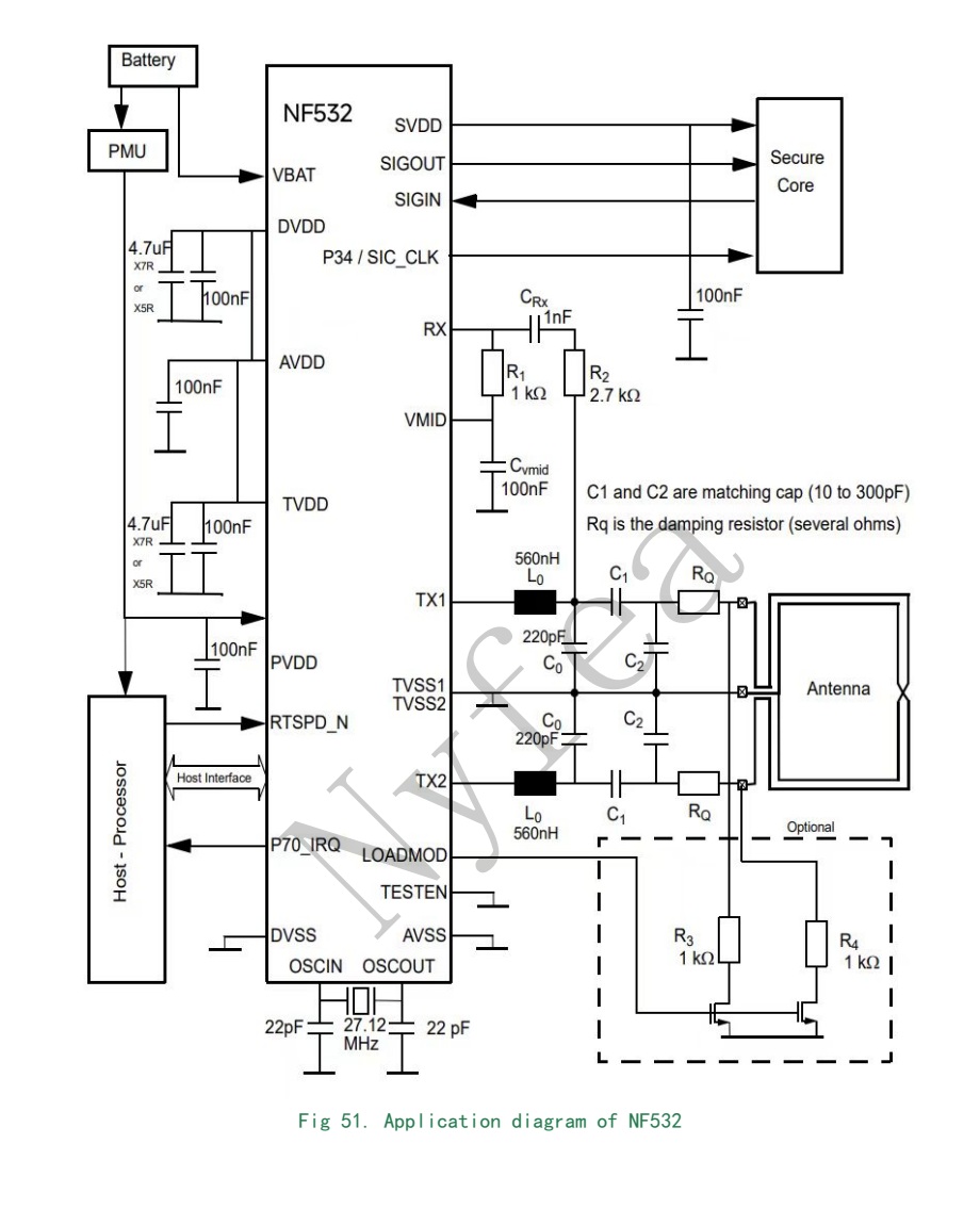
The reference circuit shows the intended supply domains, clock network, host connection and balanced RF path. Antenna matching and damping values must be recalculated and tuned on the final PCB.
HVQFN40 Package and Pinout
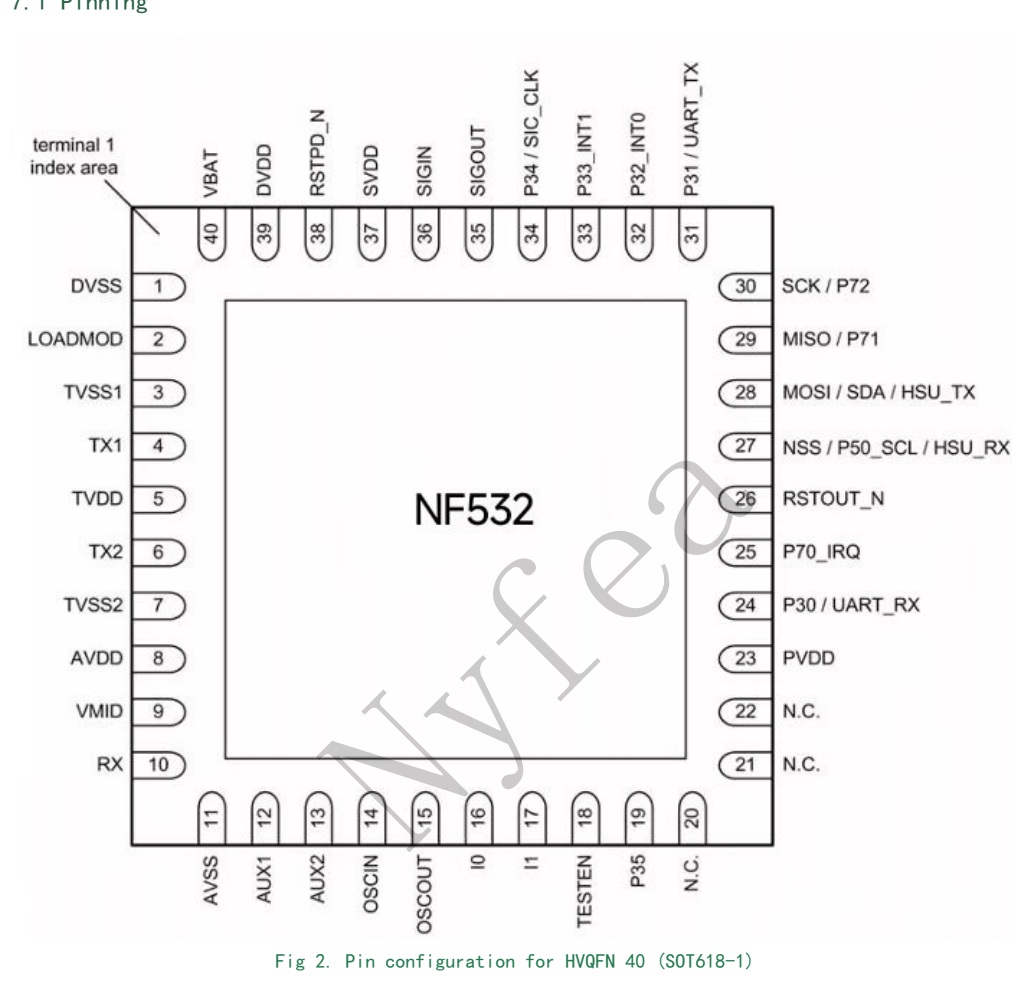
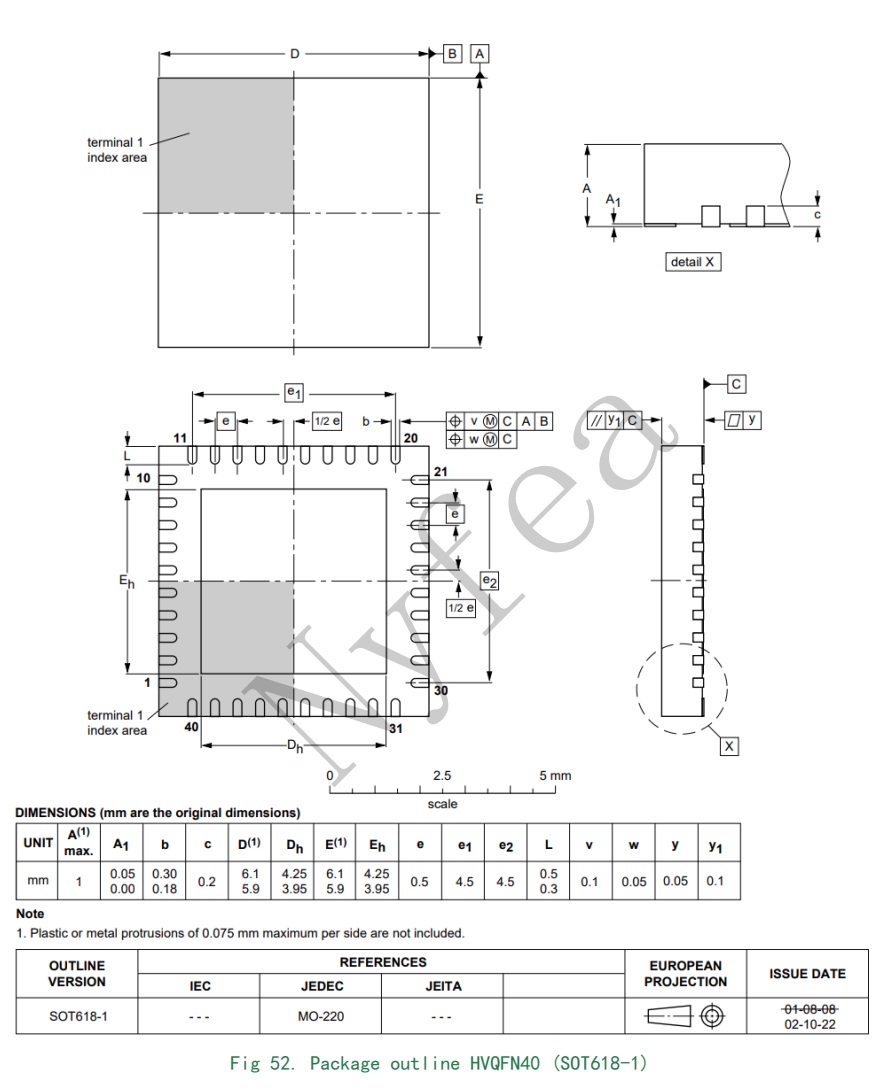
NF532 is documented in a 40-terminal HVQFN package, outline SOT618-1. The nominal body size is 6 mm × 6 mm with a maximum package height of 0.85 mm. The exposed center pad is part of the electrical and thermal design.
Application Areas
 Access controlIdentification and authorization terminals.
 NFC equipmentEmbedded contactless communication.
 Connected devicesSmart appliances and IoT equipment.
 Consumer electronicsCompact personal electronic products.
Engineering Guidance
Engineering FAQs
Does NF532 operate as both a reader and a card?
Yes. The documented modes include reader/writer operation plus Type A/MIFARE and FeliCa card-emulation modes. Firmware and external system requirements differ by mode.
Can the 50 mm or 100 mm distance be guaranteed?
No. These are typical reference values under suitable conditions. The final distance is a property of the complete RF system and target.
Can an existing NFC controller be replaced without redesign?
Do not assume pin, register, firmware, RF-network or power compatibility. Compare the complete specifications and validate production-intent hardware.
This page summarizes the supplied NF532 product specification for component evaluation. Confirm the latest controlled revision, package status, electrical limits, RF tuning and qualification requirements before production release.