
NF663 Multi-Protocol 13.56 MHz RFID Reader IC
NF663 is a highly integrated 13.56 MHz contactless reader/writer transceiver for multi-protocol HF RFID and NFC applications. It supports ISO/IEC 14443 Type A and Type B, JIS X 6319-4 (FeliCa scheme), ISO/IEC 15693, ISO/IEC 18092 passive-initiator operation, ICODE EPC, and ISO/IEC 18000-3 mode 3. The device integrates a high-output RF frontend, protocol framing and error checking, a 512-byte FIFO, 8 kB EEPROM, programmable I/O, timers, interrupts, and SPI, I²C, or UART host interfaces.
Product scope: NF663 is a board-level reader/writer IC, not a complete reader module. A finished design requires a host MCU, power circuitry, a 27.12 MHz clock, RF filtering and impedance matching, an antenna, firmware, PCB layout, interoperability testing, and application-level security. Support for an air-interface standard does not by itself establish end-product compliance or certification.
The product specification includes the register map, interface timing, low-power behavior, RF design guidance, electrical characteristics, typical application circuit, pin assignment, and SOT617-1 package dimensions. Use the current controlled document for design decisions.
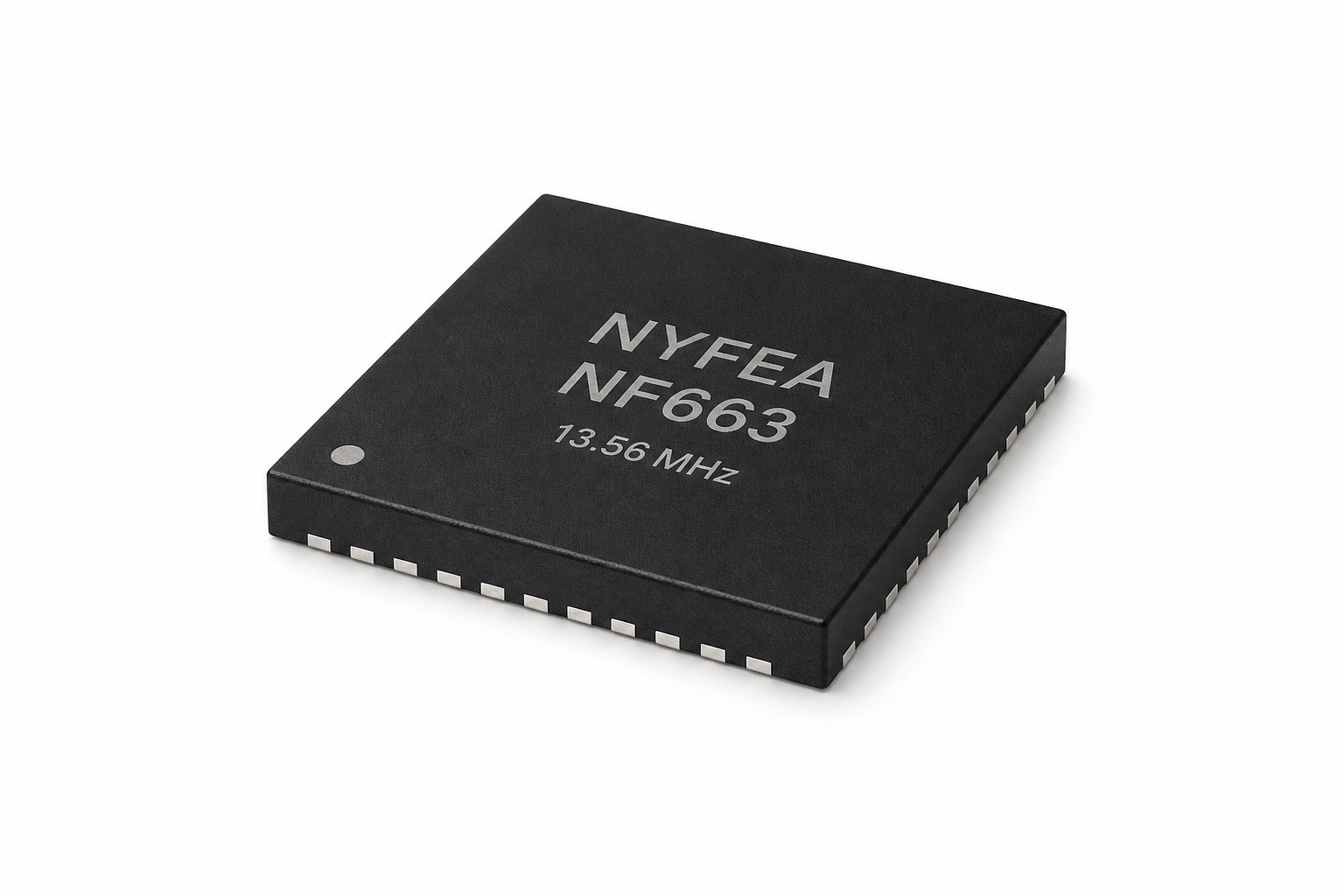
NF663 13.56 MHz Reader/Writer IC at a Glance
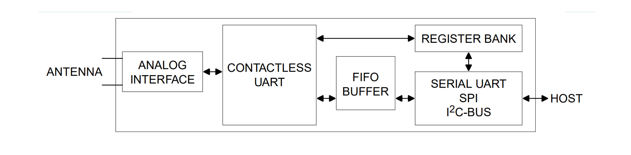
NF663 combines a 13.56 MHz transmitter, balanced receiver, contactless protocol processing, a register bank, 512-byte FIFO, host interfaces, and programmable control functions in one HVQFN32 device. It is intended for embedded readers that must communicate with several proximity, vicinity, FeliCa-scheme operation, and EPC HF card or tag families.
The integrated transmitter can directly drive a properly designed passive RF filtering and matching network; no external active device is required in the RF path. NF663 performs time-critical modulation, demodulation, framing, parity, and CRC functions, while the host processor implements higher protocol layers, application logic, and system security.
NF663 Selection Summary
| Product-selection question | NF663 capability | System-level validation required |
|---|---|---|
| Does the reader need several 13.56 MHz card and tag families? | ISO/IEC 14443 A/B, FeliCa scheme, ISO/IEC 15693, ISO/IEC 18092 passive initiator, and EPC HF modes. | Target credential interoperability, protocol software, security, and certification. |
| Does the host require a high-throughput data buffer? | 512-byte transmit/receive FIFO. | MCU service timing, interrupt strategy, and application throughput. |
| Which MCU interfaces are available? | SPI up to 10 Mbit/s, I²C up to 1000 kBd, and UART up to 1228.8 kBd. | Interface strapping, I/O voltage, firmware driver, and startup sequence. |
| Can the design connect a secure access module? | Dedicated auxiliary I²C interface for a SAM. | SAM selection, keys, cryptographic protocol, provisioning, and security certification. |
| Is low-power card detection required? | Power-down, standby, modem-off, and LPCD operating modes. | Complete-system current, antenna baseline, I/Q thresholds, false-wake rate, and wake timing. |
| What read range can the design target? | The specification states a typical read/write distance of up to 12 cm with an ISO/IEC 14443 Type A or MIFARE card, depending on antenna size and tuning. | Treat 12 cm as a data-sheet reference, not a guaranteed product range. Verify the final antenna, card or tag, orientation, enclosure, supply, EMC environment, and firmware settings. |
| Is NF663 a complete RFID reader module? | No. NF663 is a board-level reader/writer transceiver IC. | The MCU, clock, power circuitry, RF network, antenna, firmware, PCB design, and end-product approvals are external to the IC. |
Integrated Reader Architecture and Key Functions
- Multi-protocol reader/writer: ISO/IEC 14443 Type A and Type B, JIS X 6319-4 (FeliCa scheme), ISO/IEC 15693, ISO/IEC 18092 passive initiator, ICODE EPC, and ISO/IEC 18000-3 mode 3.
- High contactless data rates: up to 848 kbit/s for ISO/IEC 14443 Type A/B and up to 424 kbit/s for the FeliCa scheme.
- Integrated RF front end: high-power transmitter, balanced receiver, modulation, demodulation, framing, parity, and CRC support.
- 512-byte FIFO: supports buffered data transfer, programmable high- and low-water alerts, and reduced host-service overhead.
- 8 kB EEPROM: 64-byte pages provide areas for product configuration, reset data, user storage, MIFARE keys, and protocol register sets.
- Timers and interrupts: five timer channels support timeout, watchdog, wake-up, stopwatch, one-shot, and periodic-trigger functions; programmable interrupt sources are available on IRQ.
- Flexible host connectivity: SPI up to 10 Mbit/s, I²C/I²CL host modes, and UART up to 1228.8 kBd.
- Secure-access-module connection: dedicated auxiliary I²C interface for a SAM used as secure key storage or cryptographic coprocessor.
- Low-power operation: power-down, standby, modem-off, and low-power card detection (LPCD).
- Programmable I/O: up to eight multifunction pins for application control and signalling.
- Integrated clock resources: PLL operation from a 27.12 MHz crystal and programmable CLKOUT from 1 MHz to 24 MHz.
- MIFARE support: communication with MIFARE Classic 1K/4K, MIFARE Ultralight, MIFARE Ultralight C, MIFARE Plus, and MIFARE DESFire products, with hardware support for MIFARE Classic encryption.
- Read/write distance: the product specification states a typical distance of up to 12 cm with an ISO/IEC 14443 Type A or MIFARE card, depending on antenna size and tuning.
- Compact package: 32-terminal HVQFN, SOT617-1 outline, 5 mm × 5 mm × 0.85 mm, moisture sensitivity level 2.
EEPROM, FIFO, Timers, and Interrupt Control
NF663 integrates the memory and control resources required for host-managed contactless transactions. These resources are especially relevant when comparing reader ICs, estimating firmware workload, and defining system response time.
| Resource | NF663 implementation | Engineering use |
|---|---|---|
| EEPROM | 8 kB organized in 64-byte pages | Sections are provided for product configuration, reset data, user storage, MIFARE keys, and protocol register sets. Access rights vary by section. |
| FIFO | 512-byte transmit/receive buffer | Supports programmable WaterLevel thresholds, high- and low-water alerts, length reporting, and overflow status. |
| Timers | Five timer channels | Timer0 to Timer3 support selectable clock sources and 16-bit down-counters; Timer4 is dedicated to wake-up functions using the internal low-frequency oscillator. |
| Timer modes | Timeout, watchdog, wake-up, stopwatch, one-shot, and periodic trigger | Supports protocol timing, host supervision, low-power wake-up, and scheduled operations. |
| Interrupt controller | Two 8-bit status registers and two corresponding enable registers | Reports command completion, transmit and receive events, FIFO thresholds, communication errors, LPCD detection, start-of-frame detection, and enabled global events through IRQ. |
Multi-Protocol Capabilities and Data Rates
ISO/IEC 14443 Type A
106, 212, 424, and 848 kbit/s, including support for listed MIFARE product families.
ISO/IEC 14443 Type B
106, 212, 424, and 848 kbit/s. NF663 handles Layer 2 and Layer 3 functions except anticollision; anticollision and higher layers are implemented in host firmware.
JIS X 6319-4 (FeliCa scheme)
212 and 424 kbit/s.
ISO/IEC 18092
Passive-initiator operation at 106, 212, and 424 kbit/s.
ISO/IEC 15693
Reader-to-tag rates of 1.66 or 26.48 kbit/s and tag-to-reader rates up to 52.96 kbit/s, depending on coding and subcarrier configuration.
ICODE EPC / ISO/IEC 18000-3 Mode 3
Supports ICODE EPC UID, EPC OTP, and EPC Class-1 HF operating modes; protocol handling follows the applicable standard.
| Protocol or technology | Operating role | Supported data rate | Implementation note |
|---|---|---|---|
| ISO/IEC 14443 Type A | Reader/writer | 106 / 212 / 424 / 848 kbit/s | Protocol framing, parity, and CRC handled in the IC. |
| ISO/IEC 14443 Type B | Reader/writer | 106 / 212 / 424 / 848 kbit/s | NF663 handles Layer 2 and Layer 3 functions except anticollision; anticollision and higher layers run in the host firmware. |
| JIS X 6319-4 | Reader/writer | 212 / 424 kbit/s | FeliCa-scheme communication. |
| ISO/IEC 18092 | Passive initiator | 106 / 212 / 424 kbit/s | The initiator generates and maintains the RF carrier; the target responds by load modulation. |
| ISO/IEC 15693 | Reader/writer | Reader to tag: 1.66 / 26.48 kbit/s; tag to reader: 6.62 to 52.96 kbit/s | Available rates depend on coding and subcarrier configuration. |
| ICODE EPC / ISO/IEC 18000-3 mode 3 | Reader/writer | Protocol-defined | For compatible ICODE EPC UID, EPC OTP, and EPC Class-1 HF devices; implement the applicable standard in host firmware. |
Host Interfaces and SAM Integration
NF663 provides SPI, UART, and I²C-bus host connectivity, including the I²C and I²CL implementations described in the product specification. The interface is selected through multifunction configuration pins; verify the required strapping, I/O supply, pin assignment, and reset sequence before schematic release. A separate auxiliary I²C interface connects to a secure access module.
| Interface | Maximum rate | Primary signals | Engineering note |
|---|---|---|---|
| SPI | 10 Mbit/s | NSS, SCK, MOSI, MISO on multiplexed pins | Full-duplex synchronous host interface. |
| I²C / I²CL | 400 kBd / 1000 kBd for I²C-bus | SDA, SCL on multifunction interface pins | The product specification documents both I²C and I²CL host-interface implementations. |
| UART | 1228.8 kBd | RX, TX | UART framing is similar to RS-232, but pin voltage is logic-level and depends on the interface supply. |
| Auxiliary I²C | Application dependent | AUX1, AUX2 | Dedicated SAM connection for secure key storage or cryptographic processing. |
Power Management and Low-Power Card Detection
| Mode | Functional state | Exit or wake-up | Typical design use |
|---|---|---|---|
| Power-down | Internal circuits are switched off for minimum IC current. | Release PDOWN and perform the specified restart sequence. | Lowest-power state when full reinitialization is acceptable. |
| Standby | Low-current state with configuration retained as specified. | Host or configured wake event; typical wake-up time is 15 µs. | Fast restart between reader operations. |
| Modem-off | RF modem functions are disabled while the host interface and digital control remain available. | Re-enable modem functions through registers. | Configuration or host communication without active RF operation. |
| LPCD | The low-frequency oscillator periodically checks the antenna response using programmable I/Q thresholds. | Detected card, programmed timeout, or host control. | Duty-cycled card detection in energy-sensitive readers. |
Electrical Characteristics and Operating Limits
| Parameter | Minimum | Typical | Maximum | Unit or condition |
|---|---|---|---|---|
| VDD / PVDD | 3.0 | 5.0 | 5.5 | V, recommended operating range |
| TVDD transmitter supply | 3.0 | 5.0 | 5.5 | V, recommended operating range |
| Ambient operating temperature | −25 | — | +85 | °C |
| Storage temperature | −40 | — | +100 | °C |
| Supply current, modem on | — | 17 | 20 | mA, specified conditions |
| TVDD transmitter current | — | 100 | 200 | mA, RF load and settings dependent |
| Standby / LPCD sleep current | — | 3 | 6 | µA, specified conditions |
| Power-down current at 25 °C | — | 8 | 40 | nA, PDOWN high |
RF Front-End and Antenna Matching Design
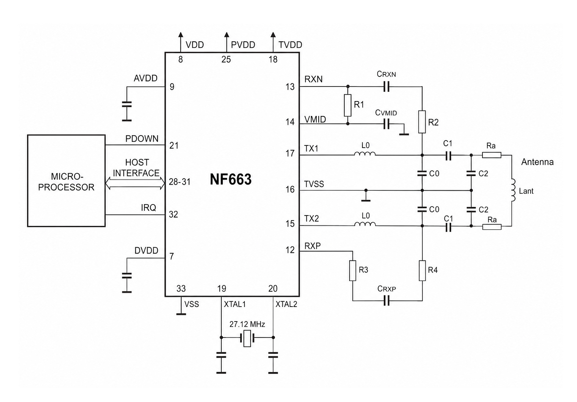
TX1 and TX2 drive the antenna network symmetrically around TVSS. The reference network contains an EMI low-pass filter followed by the impedance-matching capacitors and antenna damping elements. RXP and RXN form the balanced receive path, while VMID supplies the receiver bias reference.
For systems that require a remote or externally amplified RF assembly, NF663 also provides a digital active-antenna path through SIGOUT and SIGIN. The host can control passive and active RF paths sequentially. This function requires register-level configuration and system-specific signal-integrity, timing, EMC, and fail-safe validation.
The reference clock uses a 27.12 MHz crystal. The specification lists ±250 ppm tolerance, 10 pF load capacitance, and up to 100 Ω ESR. CLKOUT can be derived from the internal PLL and programmed from 1 MHz to 24 MHz.
- Place the crystal and load capacitors close to XTAL1 and XTAL2.
- Keep RF-current loops compact and preserve symmetry between TX1 and TX2.
- Separate RXP/RXN and VMID routing from fast digital signals and transmitter-current paths.
- Connect the exposed ground pad to a low-impedance PCB ground structure for electrical and thermal performance.
- Calculate and tune the EMI filter and matching values from the actual antenna impedance.
NF663 Reference Application Circuit
The reference circuit shows the host processor, interrupt and power-down controls, separated supply functions, 27.12 MHz crystal, balanced TX1/TX2 transmitter, RXP/RXN receiver, VMID network, EMI filter, matching components, and antenna. The diagram below is directly reproduced from the NF663 product specification and only enhanced for display clarity.
HVQFN32 Pinout, Ground Pad, and Package Dimensions
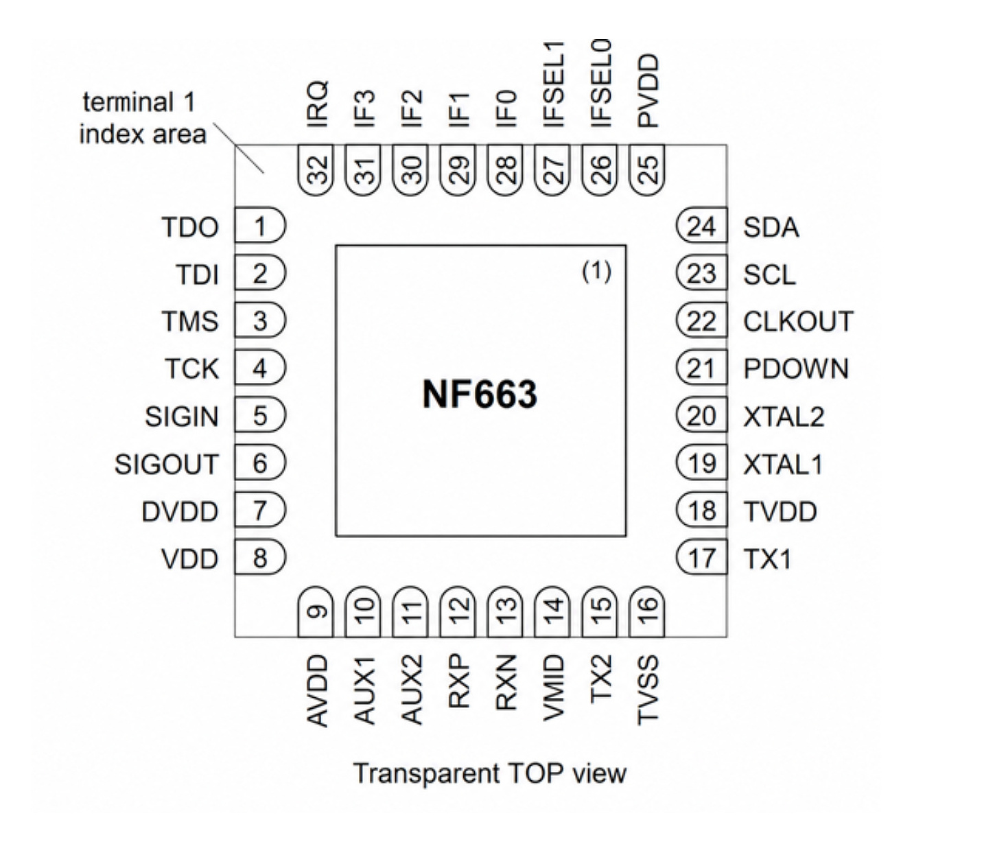
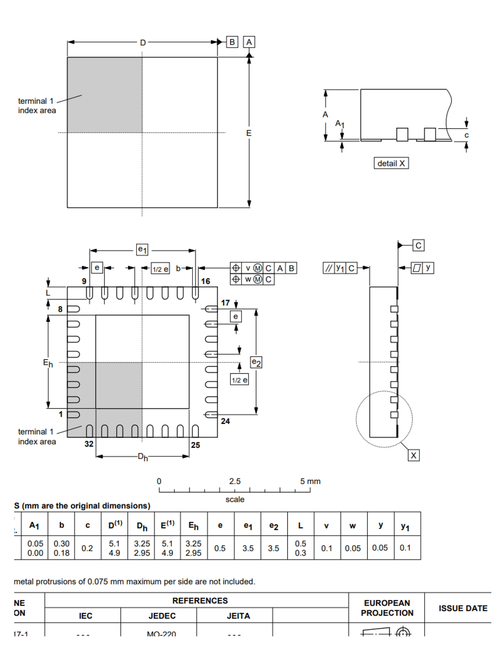
NF663 is supplied in a 32-terminal HVQFN package with an exposed center pad identified as terminal 33. The exposed pad must be connected to VSS and incorporated into the PCB thermal and grounding design. The package outline is SOT617-1 with a nominal 5 mm × 5 mm body and 0.5 mm terminal pitch.
| Item | Specification | PCB and assembly note |
|---|---|---|
| Type number | NF663 | The ordering table lists NF663 in the HVQFN32 package. |
| Package outline | HVQFN32, SOT617-1 | 32 perimeter terminals plus exposed ground/thermal pad. |
| Nominal body | 5 mm × 5 mm × 0.85 mm | Use the complete tolerance table for land-pattern design. |
| Terminal pitch | 0.5 mm | Review solder-mask, paste, stencil, and inspection capabilities. |
| Moisture sensitivity | MSL 2 | Specified for 260 °C convection reflow; follow dry-pack and floor-life requirements. |
| Reference crystal | 27.12 MHz | Place close to XTAL1/XTAL2 and control parasitics. |
NF663 Target Applications and Selection Guidance
NF663 is intended for multi-protocol 13.56 MHz readers that need broad card and tag coverage, host-controlled protocol processing, a 512-byte FIFO, nonvolatile configuration storage, optional SAM connectivity, and low-power card detection.
 Industrial and Logistics HF RFIDISO/IEC 15693 and EPC HF identification, configuration, and traceability readers.
 Access Control and Identity ReadersMulti-technology terminals using supported proximity and vicinity credentials.
 Transit and TicketingReader designs for FeliCa-scheme operation, MIFARE, and ISO/IEC 14443 card environments.
 Contactless TerminalsISO/IEC 14443 Type A/B terminals requiring controlled RF implementation.
 Embedded NFC DevicesISO/IEC 18092 passive-initiator and multi-protocol reader applications.
NF663 RFID Reader IC Engineering FAQs
What is an RFID reader IC?
An RFID reader IC is the RF and baseband semiconductor at the core of a contactless reader. It generates and modulates the 13.56 MHz field, receives the card or tag response, performs protocol framing and error checking, and exchanges commands and data with a host microcontroller.
What does an RFID reader chip do?
An RFID reader chip converts host commands into protocol-compliant contactless transactions and returns decoded card or tag data. Depending on the device, it may integrate the RF driver and receiver, framing logic, parity and CRC processing, FIFO memory, host interfaces, timers, interrupts, nonvolatile memory, and low-power card detection.
What is the difference between an RFID reader IC and an RFID reader module?
An RFID reader IC is a board-level semiconductor that requires external power circuitry, a host controller, clock components, an RF matching network, and an antenna. A reader module normally integrates the IC with some or all of these elements and may also include firmware. An IC provides greater control over cost, size, RF performance, and system architecture; a module generally reduces integration effort.
What is the difference between an NFC reader IC and an NFC controller?
An NFC reader IC, often called an NFC frontend, primarily implements the contactless RF interface and protocol framing under host control. An NFC controller typically adds an embedded NFC firmware stack and a standardized host interface. Product terminology varies, so selection should be based on supported operating modes, host-software responsibilities, interfaces, security architecture, and qualification requirements.
Which RFID reader IC should I choose?
Select an RFID reader IC by the required air-interface standards, data rates, RF output capability, host interface, buffer and memory resources, low-power behavior, package, temperature range, software architecture, and certification plan. NF663 is intended for multi-protocol 13.56 MHz reader/writer designs that require a 512-byte FIFO, 8 kB EEPROM, up to eight programmable I/O pins, SPI, I²C or UART connectivity, and an optional SAM interface.
What is the NF663 RFID reader IC?
NF663 is a highly integrated 13.56 MHz multi-protocol contactless reader/writer transceiver IC. It combines a high-output RF frontend, protocol framing, parity and CRC processing, a 512-byte FIFO, 8 kB EEPROM, host interfaces, programmable I/O, timers, interrupts, and low-power card detection in a 32-terminal HVQFN package.
Which contactless standards does NF663 support?
NF663 supports reader/writer operation for ISO/IEC 14443 Type A and Type B, JIS X 6319-4 (FeliCa scheme), ISO/IEC 15693, ICODE EPC UID and EPC OTP, and ISO/IEC 18000-3 mode 3 / EPC Class-1 HF. It also supports ISO/IEC 18092 passive-initiator operation at 106, 212, and 424 kbit/s.
What is the difference between NF663 and NF522?
NF663 targets broader multi-protocol reader designs. In addition to ISO/IEC 14443 Type A/B and ISO/IEC 15693 support, it provides FeliCa-scheme operation, ISO/IEC 18092 passive-initiator, and EPC HF modes, together with a 512-byte FIFO, 8 kB EEPROM, and a dedicated SAM interface. NF522 is a separate product; do not assume pin, register, firmware, power, or RF-network compatibility.
Can NF663 directly replace CLRC663?
The NF663 product specification supplied for this page does not claim drop-in compatibility with CLRC663. Before considering a substitution, compare the complete pinout, exposed-pad connection, supply architecture, interface-mode selection, register map, EEPROM contents, command behavior, firmware, RF matching network, electrical limits, package tolerances, and qualification requirements. Treat the substitution as a controlled redesign until it has been verified on production-intent hardware.
Can NF663 directly replace MFRC522?
Do not assume a drop-in replacement. NF663 has a different multi-protocol feature set, interface and memory architecture, pinout, power requirements, register behavior, and RF network. Migration from MFRC522 requires schematic and PCB review, firmware adaptation, antenna retuning, interoperability testing, and complete system validation.
Which host interfaces are available on NF663?
NF663 supports SPI at up to 10 Mbit/s, I²C at up to 400 kBd in Fast mode and 1000 kBd in Fast-mode Plus, and UART at up to 1228.8 kBd. The host-interface pins also support an I²CL implementation described in the product specification. A separate auxiliary I²C interface is provided for a secure access module.
What contactless data rates does NF663 support?
NF663 supports 106, 212, 424, and 848 kbit/s for ISO/IEC 14443 Type A and Type B; 212 and 424 kbit/s for the FeliCa scheme; and 106, 212, and 424 kbit/s in ISO/IEC 18092 passive-initiator mode. ISO/IEC 15693 supports 1.66 and 26.48 kbit/s from reader to tag and 6.62/6.67, 13.24, 26.48/26.69, and 52.96 kbit/s from tag to reader, depending on coding and subcarrier configuration.
What read range can NF663 achieve?
The product specification states a typical read/write distance of up to 12 cm with an ISO/IEC 14443 Type A or MIFARE card, depending on antenna size and tuning. This is not a guaranteed system specification. Actual range depends on the antenna geometry and Q factor, matching, transmitter supply, card or tag design, orientation, PCB layout, enclosure, nearby materials, noise, and firmware settings.
Does NF663 support low-power card detection?
Yes. NF663 supports low-power card detection (LPCD), standby, power-down, and modem-off modes. The specification lists 3 µA typical standby and LPCD sleep current and 8 nA typical power-down current at 25 °C under the stated test conditions. These figures apply to the IC; total product standby current also includes the host, regulator, antenna network, and other loads.
Is NF663 EMV contactless certified?
The NF663 product specification states that RF-level compliance with the EMV contactless protocol specification can be achieved. This statement is not a certification claim for NF663 or for a finished payment terminal. The complete reader must be designed, measured, and submitted through the applicable approval process.
Can the reference antenna component values be copied directly into production?
No. The reference circuit defines the RF topology, including the EMI filter, matching network, damping elements, and balanced receive connection. Component values must be calculated and tuned for the actual antenna, PCB, enclosure, supply, target cards or tags, and compliance objectives. The product specification warns against reusing values from another reader IC without adjustment.
This page summarizes the NF663 product specification for product evaluation and engineering reference. It does not replace the complete controlled specification. Confirm the current revision, register definitions, pin configuration, interface timing, absolute maximum ratings, RF network, PCB layout, thermal design, assembly process, and qualification requirements before production release.
Download NF663 Product Specification Contact NYFEA for Product Support