
SN74LVC1G06 Open-Drain Inverter
NYFEA SN74LVC1G06 is a single inverting buffer and driver with an open-drain output, specified for 1.65 V to 5.5 V VCC operation. Input A and open-drain output Y accept 0 V to 5.5 V, Ioff supports partial-power-down applications, and SOT23-5 and SC70-5 package options are listed.
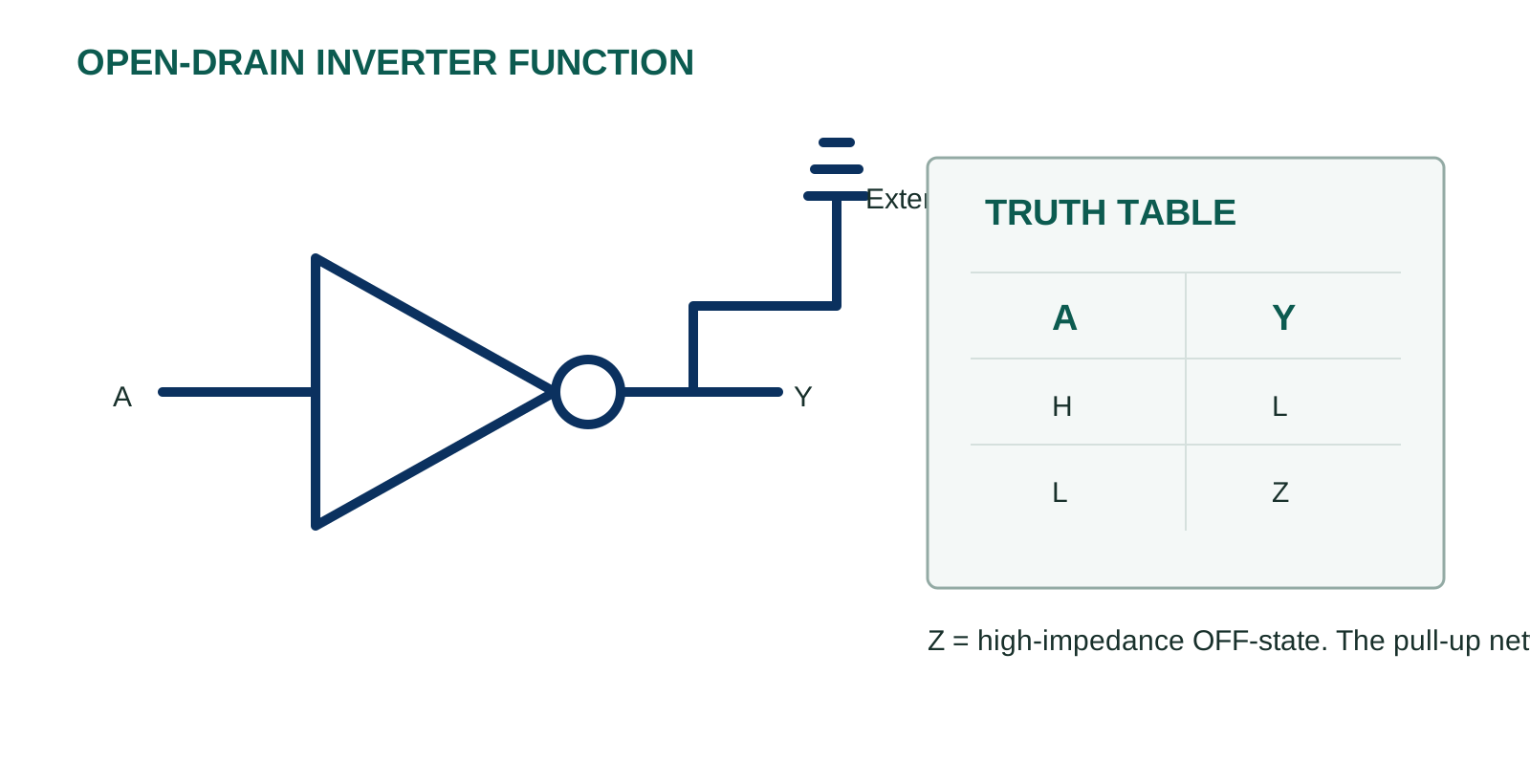
Product scope: A HIGH input turns the output transistor on and pulls Y LOW. A LOW input turns the transistor off and leaves Y in the high-impedance state. An external pull-up resistor is required to create a valid HIGH level; the device does not source output current.
Use the current controlled PDF for threshold limits, output loading, switching conditions, package tolerances, tape orientation and production-release decisions.
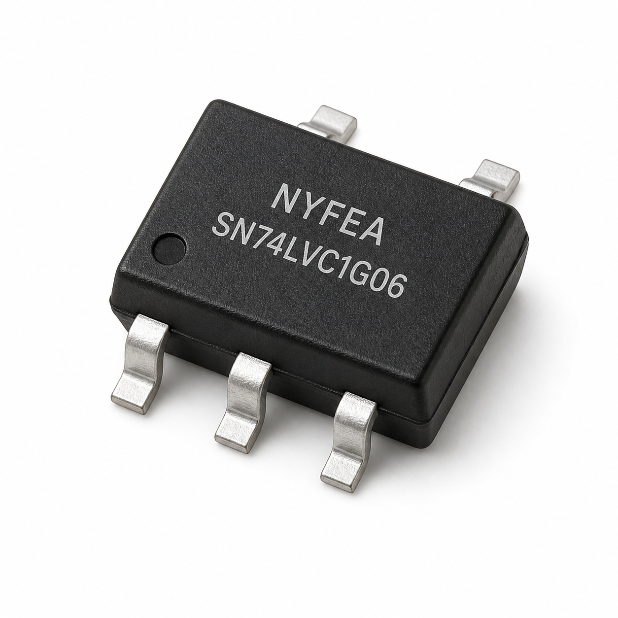
Product Overview and Selection Scope
SN74LVC1G06 combines one inverting input stage with an open-drain NMOS output. It can pull a shared node LOW but cannot actively drive it HIGH. The specified VCC operating range is 1.65 V to 5.5 V, and both input A and output Y accept 0 V to 5.5 V under the recommended conditions.
Output architecture
When A is HIGH, Y is pulled LOW. When A is LOW, Y becomes high impedance and the external pull-up network establishes the HIGH level.
Wired logic
Multiple compatible open-drain outputs may share one pull-up to implement active-low wired-OR or active-high wired-AND behavior.
Partial power-down
Ioff is specified with VCC = 0 V and VI or VO = 5.5 V, limiting current through the powered-down device path.
Package choice
SOT23-5 and SC70-5 share the same pin assignment but have different footprints, markings and thermal impedances.
Selection boundary: The PDF does not specify Schmitt-trigger hysteresis, an internal pull-up, a guaranteed pull-up resistor value, tri-state control independent of A, or end-product qualification. Pull-up voltage, resistance, bus capacitance, LOW-state sink current, rise time and static power are system design responsibilities.
Logic Function, Truth Table and Pin Assignment
The logical inversion is implemented through an open-drain output: A = H produces Y = L, while A = L produces Y = Z. The external pull-up converts Z into a usable HIGH level.
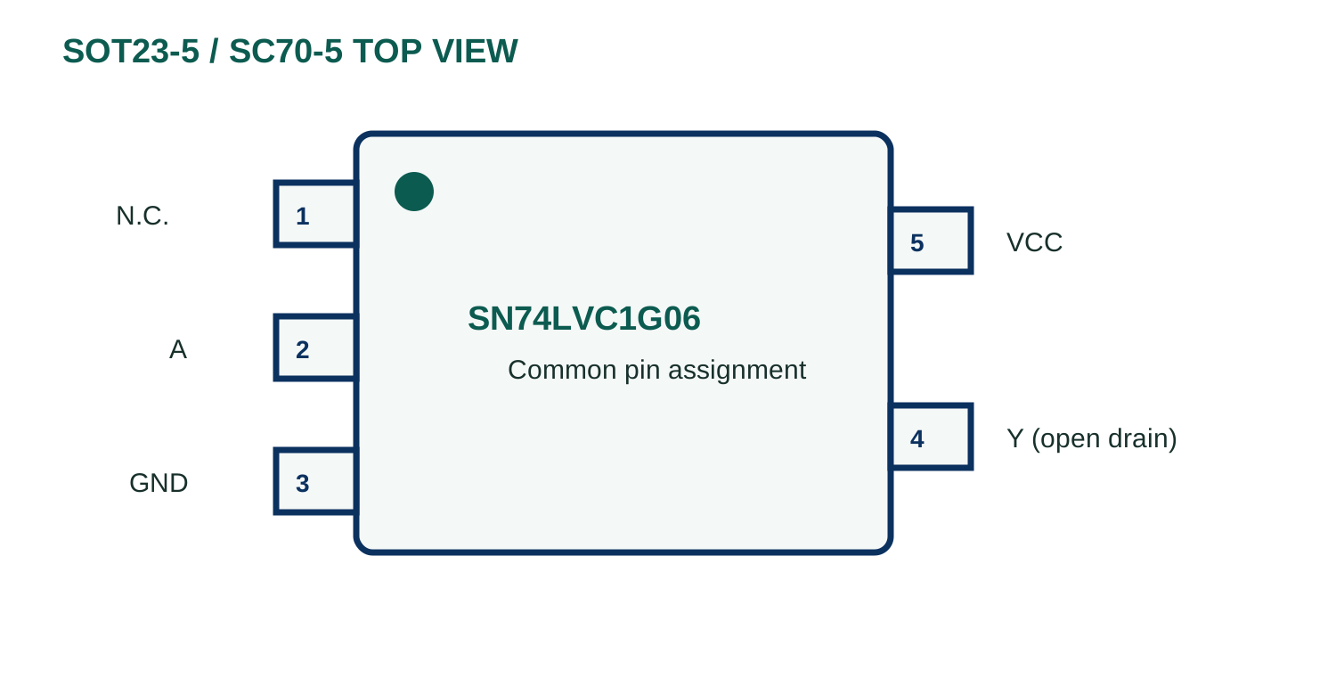
| Pin | Name | Type | Function | Engineering note |
|---|---|---|---|---|
| 1 | N.C. | - | Not connected | Do not use as a signal or supply connection. |
| 2 | A | Input | Inverting logic input | Hold at VCC or GND when unused. |
| 3 | GND | Power | Ground | Use a short return to the bypass capacitor and LOW-current path. |
| 4 | Y | Output | Open-drain output | Requires an external pull-up; may share a node only with compatible open-drain outputs. |
| 5 | VCC | Power | Supply | Place local decoupling close to pins 5 and 3. |
Ordering Codes and Package Selection
| Ordering number | Temperature range | Package | Top marking | MSL | Packing |
|---|---|---|---|---|---|
| SN74LVC1G06DCKR | -40 °C to +125 °C | SC70-5 / SOT353 equivalent | CT5 | MSL 3 | Tape and reel, 3,000 units |
| SN74LVC1G06DBVR | -40 °C to +125 °C | SOT23-5 | C06J | MSL 3 | Tape and reel, 3,000 units |
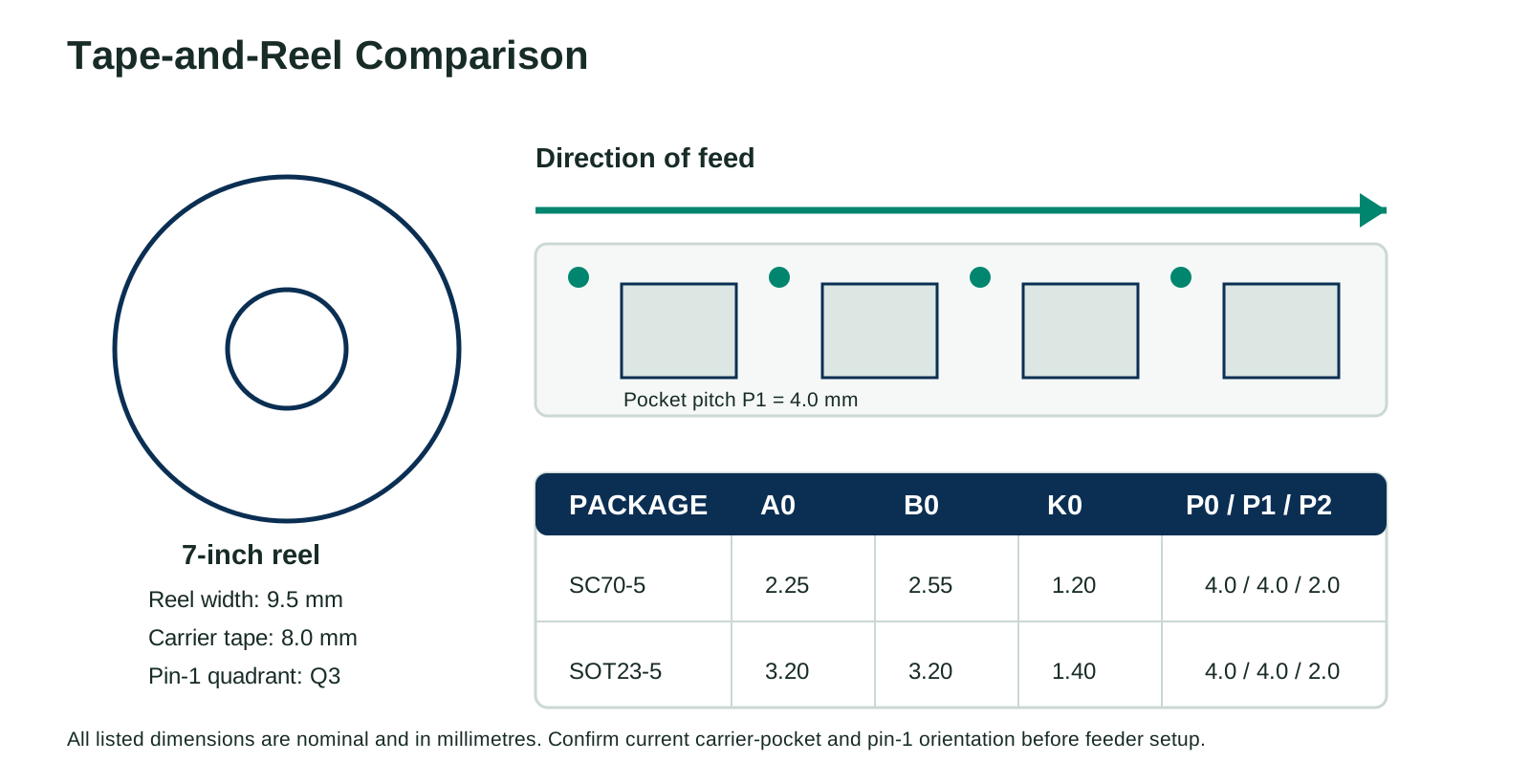
Additional lot, date, vendor, logo or environmental markings may appear. Confirm the full order code, package dimensions, marking and reel orientation during receiving inspection.
Recommended Operating Conditions and Absolute Limits
Recommended operating conditions define the functional design range. Absolute maximum ratings are stress limits only and do not establish normal operation or long-term reliability.
| Parameter | Condition | Minimum | Maximum | Unit |
|---|---|---|---|---|
| Supply voltage, VCC | Operating | 1.65 | 5.5 | V |
| Supply voltage, VCC | Data retention only | 1.5 | - | V |
| High-level input, VIH | VCC = 1.65 to 1.95 / 2.3 to 2.7 / 3.0 to 3.6 / 4.5 to 5.5 V | 0.65 × VCC / 1.7 / 2.2 / 0.7 × VCC | - | V |
| Low-level input, VIL | Same four VCC ranges | - | 0.15 × VCC / 0.3 / 0.4 / 0.15 × VCC | V |
| Input voltage, VI | Operating | 0 | 5.5 | V |
| Open-drain output voltage, VO | Operating | 0 | 5.5 | V |
| Input rise/fall, tr or tf | VCC = 1.8 V ±0.15 V or 2.5 V ±0.2 V | - | 20 | ns/V |
| Input rise/fall, tr or tf | VCC = 3.3 V ±0.3 V | - | 10 | ns/V |
| Input rise/fall, tr or tf | VCC = 5 V ±0.5 V | - | 5 | ns/V |
| Ambient temperature, TA | Operating | -40 | 125 | °C |
Absolute maximum and handling limits
| Parameter | Condition | Minimum | Maximum | Unit |
|---|---|---|---|---|
| Supply voltage | VCC | -0.5 | 6.5 | V |
| Input voltage | VI | -0.5 | 6.5 | V |
| Output voltage | High-impedance, power-off, or LOW state | -0.5 | 6.5 | V |
| Input clamp current | VI < 0 V | -50 | mA | |
| Output clamp current | VO < 0 V | -50 | mA | |
| Continuous output current | IO | ±50 | mA | |
| Continuous VCC or GND current | - | ±100 | mA | |
| Junction temperature | TJ | -65 | 150 | °C |
| Storage temperature | Tstg | -65 | 150 | °C |
DC Characteristics and Logic Levels
Full-range limits apply from -40 °C to +125 °C unless otherwise stated. Typical values are at +25 °C. The device specification lists only LOW-state output limits because the open-drain output does not source a HIGH level.
| VCC range | VIH minimum | VIL maximum | Engineering interpretation |
|---|---|---|---|
| 1.65 V to 1.95 V | 0.65 × VCC | 0.15 × VCC | Thresholds scale with supply. |
| 2.3 V to 2.7 V | 1.7 V | 0.3 V | Use the fixed guaranteed limits. |
| 3.0 V to 3.6 V | 2.2 V | 0.4 V | Use the fixed guaranteed limits. |
| 4.5 V to 5.5 V | 0.70 × VCC | 0.15 × VCC | Thresholds scale with supply. |
LOW output, leakage and supply current
| Parameter | Test condition | VCC | Temperature | Limit or typical value | Unit |
|---|---|---|---|---|---|
| VOL | IOL = 100 µA | 1.65 V to 5.5 V | Full | Maximum 0.1 V | V |
| VOL | IOL = 4 / 8 / 16 / 24 / 32 mA | 1.65 / 2.3 / 3.0 / 3.0 / 4.5 V | Full | Maximum 0.45 / 0.30 / 0.40 / 0.55 / 0.55 V | V |
| II | A = 5.5 V or GND | 0 V to 5.5 V | +25 °C / Full | Typical ±0.1 µA / maximum ±5 µA | µA |
| Ioff | VI or VO = 5.5 V | 0 V | +25 °C / Full | Typical ±0.1 µA / maximum ±10 µA | µA |
| ICC | VI = 5.5 V or GND, IO = 0 | 1.65 V to 5.5 V | +25 °C / Full | Typical 0.1 µA / maximum 10 µA | µA |
| ΔICC | A = VCC - 0.6 V | 3 V to 5.5 V | Full | Maximum 500 µA | µA |
AC Switching and Test Conditions
The Rev A.1 PDF lists typical propagation-delay values over the full -40 °C to +125 °C range under the stated resistor and capacitive loads. Pull-up resistance, total node capacitance and receiving threshold additionally determine the actual rising edge in an application.
| Parameter | VCC | Load condition | Temperature | Typical value | Unit |
|---|---|---|---|---|---|
| Propagation delay, tpd | 1.8 V ±0.15 V | CL = 30 pF, RL = 1 kΩ | Full | 6.4 | ns |
| Propagation delay, tpd | 2.5 V ±0.2 V | CL = 30 pF, RL = 500 Ω | Full | 4.5 | ns |
| Propagation delay, tpd | 3.3 V ±0.3 V | CL = 50 pF, RL = 500 Ω | Full | 4.2 | ns |
| Propagation delay, tpd | 5.0 V ±0.5 V | CL = 50 pF, RL = 500 Ω | Full | 3.7 | ns |
| Input capacitance, Ci | 3.3 V | VI = VCC or GND | +25 °C | 4 | pF |
| Power-dissipation capacitance, Cpd | 1.8 / 2.5 / 3.3 / 5.0 V | f = 10 MHz | +25 °C | 3 / 3 / 4 / 6 | pF |
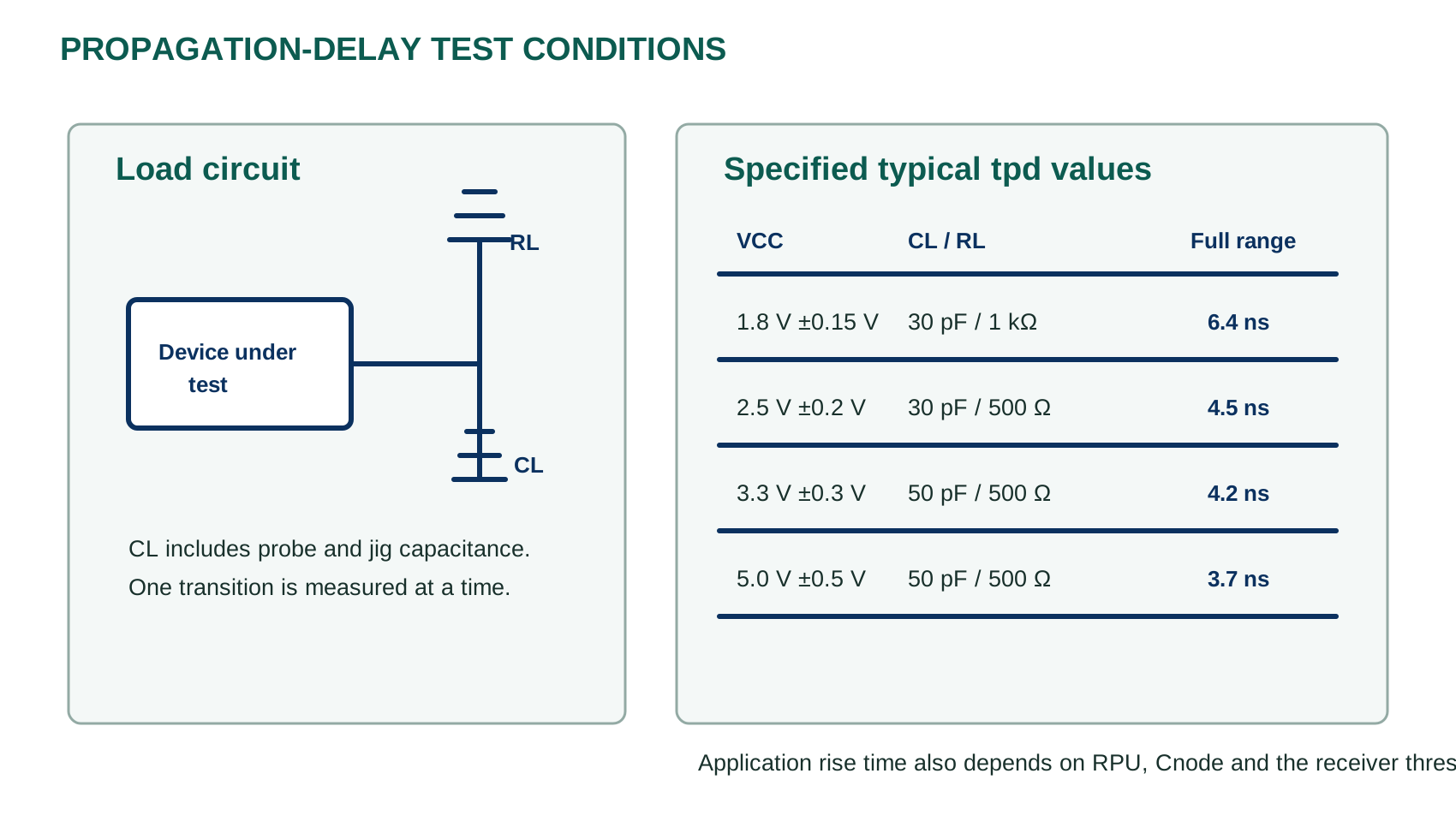
Timing boundary: The PDF provides typical values but no guaranteed maximum propagation delay or bus rise-time limit. Do not infer a guaranteed maximum frequency. Measure the finished node across voltage, capacitance, resistor tolerance and temperature.
Pull-Up Design, Power Integrity and PCB Layout
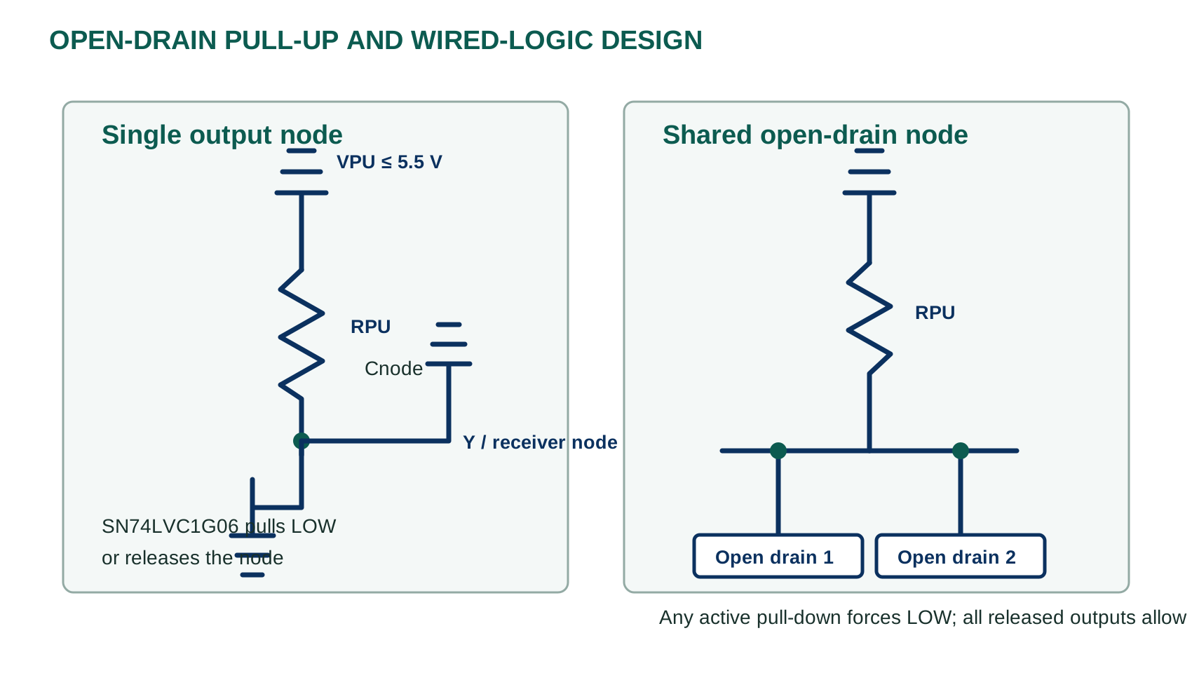
The following circuits are application-design guidance, not guaranteed reference circuits defined by the product specification. Use the PDF limits and validate the complete pull-up network, receiving threshold, wiring capacitance and power sequence.
| Design check | First-order relation | Required validation |
|---|---|---|
| LOW-state sink current | IOL ≈ (VPU - VOL) / RPU | Keep IOL within the stated VOL test-current conditions and receiver VIL margin. |
| Released-node rise | τ ≈ RPU × Cnode | Use the receiver threshold and system timing budget; the PDF does not guarantee a bus rise time. |
| Static LOW power | P ≈ VPU² / RPU | Include resistor dissipation and device sink power at maximum LOW duty cycle. |
| Shared wired node | Any active pull-down forces LOW | Only compatible open-drain outputs may share the node; never connect a push-pull HIGH driver. |
- Keep VPU within the output range: recommended VO is 0 V to 5.5 V, independent of the lower VCC used for the input stage.
- Do not leave A floating: the PDF requires every unused input to be held at VCC or GND.
- Place local bypassing close to the device: use a short VCC-to-GND loop and confirm the board PDN.
- Route the shared node compactly: connector, cable, probe and input capacitance all increase Cnode and slow the released edge.
- Validate partial power-down: Ioff limits the device path, while the pull-up and other components can still create system back-power routes.
SOT23-5 and SC70-5 Packages, Land Patterns and Packing
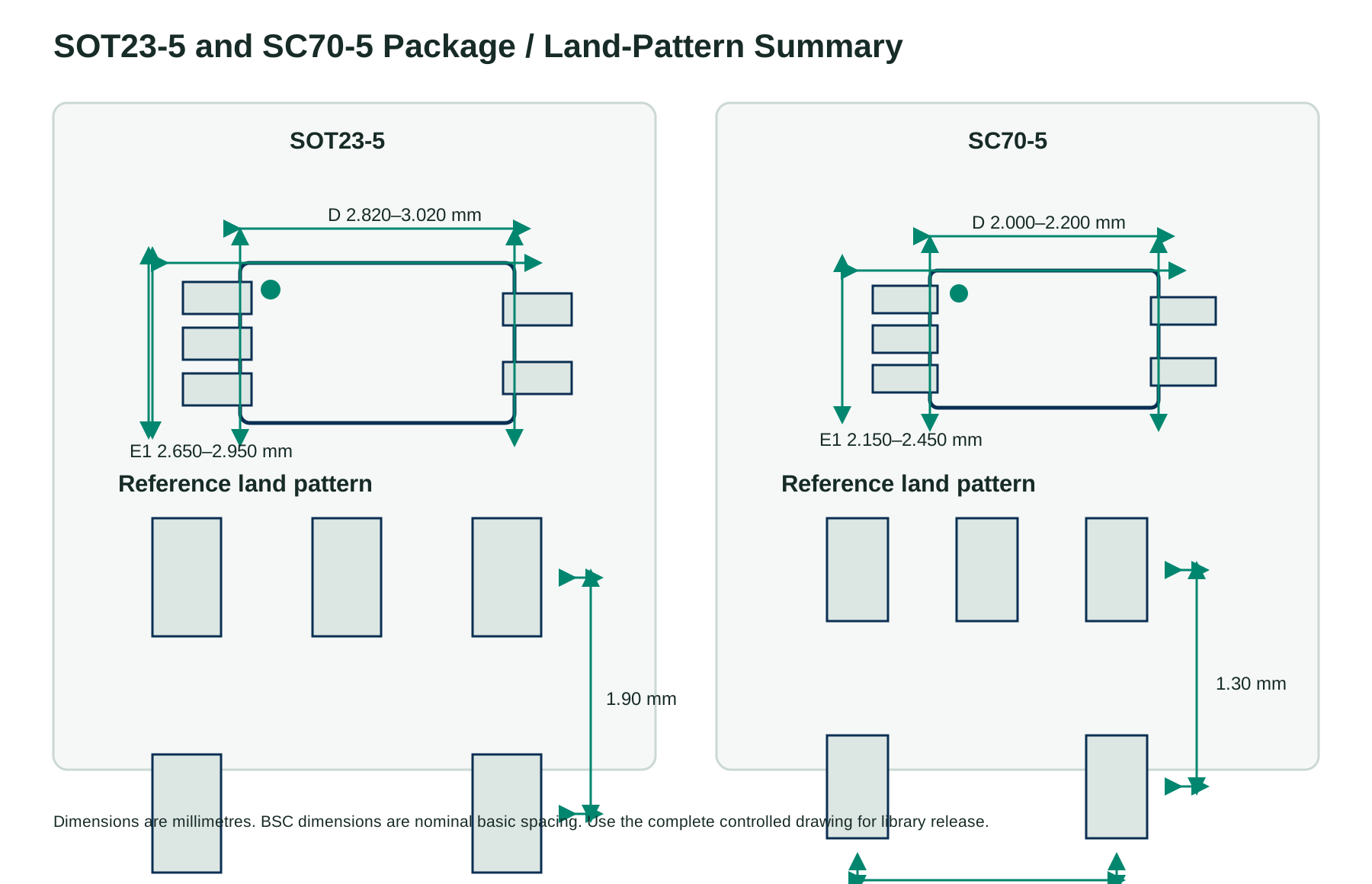
Both green package options share the same pin assignment but use different body dimensions, lead pitch, top marking and thermal impedance. Do not substitute one footprint for the other.
| Dimension | SOT23-5 | SC70-5 | Unit |
|---|---|---|---|
| Overall height A | 1.050 to 1.250 | 0.900 to 1.100 | mm |
| Body length D | 2.820 to 3.020 | 2.000 to 2.200 | mm |
| Body width E | 1.500 to 1.700 | 1.150 to 1.350 | mm |
| Overall lead span E1 | 2.650 to 2.950 | 2.150 to 2.450 | mm |
| Lead pitch e | 0.950 BSC | 0.650 BSC | mm |
| Outer lead pitch e1 | 1.800 to 2.000 | 1.300 BSC | mm |
| Lead width b | 0.300 to 0.500 | 0.150 to 0.350 | mm |
| Lead thickness c | 0.100 to 0.200 | 0.080 to 0.150 | mm |
| Lead length L | 0.300 to 0.600 | 0.260 to 0.460 | mm |
Application Guidance and Design Limitations
The Rev A.1 specification lists Blu-ray players and home theaters, desktop or notebook PCs, digital video cameras, mobile phones, personal navigation devices and portable media players. In these systems, the device can invert a control signal, level-shift through an external pull-up within the 5.5 V output limit, or combine compatible open-drain sources. These are use contexts, not end-product approvals.
 Blu-ray and Home TheaterCombine active-low status or control lines after selecting the pull-up for sink current and edge rate.
 Desktop and Notebook PCsUse for board-level reset, interrupt or status inversion where an open-drain shared node is appropriate.
 Digital Video CamerasInvert low-speed digital control signals while validating pull-up voltage, capacitance and timing.
 Mobile PhonesEvaluate compact open-drain control paths with complete standby-current and power-sequencing checks.
 Personal Navigation DevicesUse on local status or control nodes after system-level EMC, timing and pull-up validation.
SN74LVC1G06 Engineering FAQs
What logic function does SN74LVC1G06 implement?
It is an inverting open-drain buffer. A HIGH input pulls Y LOW; a LOW input releases Y into the high-impedance state.
What supply range is recommended?
VCC is specified from 1.65 V to 5.5 V for operation. The PDF separately lists 1.5 V as the minimum data-retention supply; data retention does not establish normal logic operation.
Does SN74LVC1G06 require an external pull-up?
Yes. The open-drain output can pull LOW or release the node; it cannot drive HIGH. Choose the pull-up from the required VOL, sink current, capacitance, rise time and static power.
Can the pull-up voltage differ from VCC?
The recommended output range is 0 V to 5.5 V, so a pull-up within that limit can support system-level voltage translation. Verify receiver thresholds, current, timing and sequencing in the complete circuit.
Can multiple outputs share one node?
Compatible open-drain outputs may share a pull-up for wired logic. Do not connect a push-pull output that may actively drive HIGH to the same node.
What propagation-delay values are listed?
Typical full-range tpd values are 6.4 ns at 1.8 V, 4.5 ns at 2.5 V, 4.2 ns at 3.3 V and 3.7 ns at 5 V under the stated loads. No guaranteed maximum is listed.
What does Ioff provide?
Ioff is specified with VCC = 0 V and VI or VO = 5.5 V, with ±10 µA maximum over the full temperature range. It limits the device path but does not eliminate other board-level back-power routes.
Which package should be selected?
SN74LVC1G06DBVR is SOT23-5 with C06J marking. SN74LVC1G06DCKR is SC70-5 with CT5 marking. Both are MSL 3 and packed 3,000 units per reel.
Can input A be left open?
No. The PDF explicitly requires unused inputs to be held at VCC or GND. Pin 1 is N.C. and should not be used as a functional connection.
Do the listed applications establish product certification?
No. The application list identifies possible use contexts only. Qualification, safety, EMC, reliability and production validation remain system responsibilities.
This page summarizes the SN74LVC1G06 Rev A.1 product specification for component evaluation and engineering reference. It does not replace the complete controlled specification. Confirm the current revision, ordering code, marking, pin assignment, pull-up design, logic limits, absolute maximum ratings, DC and AC conditions, package tolerances, PCB layout, assembly process and qualification requirements before production release.
