
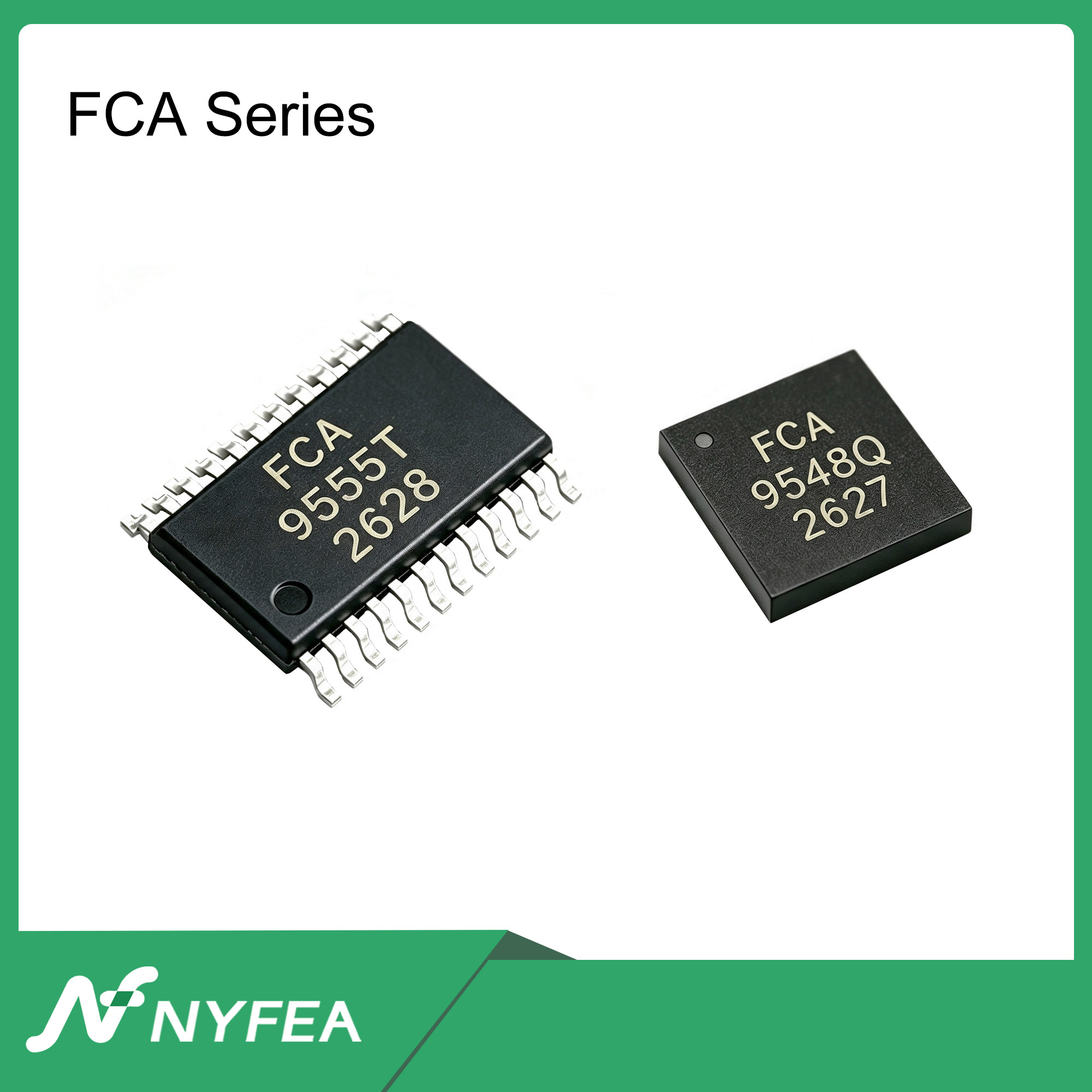
FCA Series Interface ICs Overview
Interface ICs are integrated circuits used to establish electrical connections and data paths between a host controller and peripheral devices. Depending on the interface standard and system requirements, these ICs may perform functions such as data transmission and reception, signal buffering, protocol bridging, bus switching, logic-level adaptation, and port expansion. These functions enable devices to exchange information under specified electrical conditions and communication timing requirements. Because the functions of interface ICs vary significantly by device type, product selection should be based on the target bus, signal direction, communication speed, and system interconnection architecture.
The FCA Series includes the FCA8574, FCA9535, FCA9539, FCA9555, FCA9548, and other interface ICs, covering I²C I/O expanders and I²C/SMBus bus switches. These devices can be used to expand processor GPIO resources, manage multiple downstream I²C buses, resolve slave-address conflicts, and interconnect segmented I²C buses operating at different supply voltages.
The FCA8574 provides an 8-bit quasi-bidirectional I/O port without a dedicated direction-control register. Output states are controlled by writing data to the port, while input states are obtained by reading the port. The FCA9535, FCA9539, and FCA9555 provide 16-bit GPIO ports, with each I/O pin independently configurable as an input or output through registers. Depending on the model, these devices support hardware address selection, input-state reading, output latching, and an active-low, open-drain interrupt output. The FCA9539 also provides an active-low hardware reset input.
The FCA9548 is an 8-channel bidirectional I²C/SMBus switch that allows one or more downstream channels to be selected through a control register. It connects one upstream pair of SDA and SCL lines to eight downstream buses and is suitable for systems containing multiple I²C slave devices with identical addresses, requiring bus segmentation, or requiring the isolation of faulty channels. When separate pull-up supplies are used for individual channels, the device can interconnect I²C buses operating at different logic voltages under the conditions specified in the datasheet. The FCA9548 also provides an active-low reset input that resets the I²C state machine and deselects all downstream channels.
The FW28E17Q is an interface IC but is not part of the FCA Series. It is a 1-Wire slave-to-I²C master communication bridge that converts data received over a 1-Wire bus into I²C master transactions. It can be used to control remote I²C sensors, display controllers, analog-to-digital converters (ADCs), digital-to-analog converters (DACs), and other I²C slave devices. The device includes a factory-programmed, unique 64-bit 1-Wire ROM ID, supports sleep and wake-up functions, and provides busy-status and communication-error indications. It is suitable for systems with limited GPIO resources or applications requiring remote I²C peripherals to be connected through a 1-Wire bus.
FCA Series and FW interface ICs can be used in servers, routers, communications equipment, industrial automation systems, remote sensor nodes, and other electronic products with limited interface resources. Device selection should take into account the interface type, number of GPIOs, port architecture, number of bus channels, device address, supply voltage, communication speed, operating temperature range, and package dimensions.
I²C, SMBus, and 1-Wire buses, as well as open-drain interrupt signals, typically require external pull-up resistors selected according to bus capacitance, communication speed, and supply voltage. Detailed connection requirements and electrical limitations are provided in the official datasheet for each device.
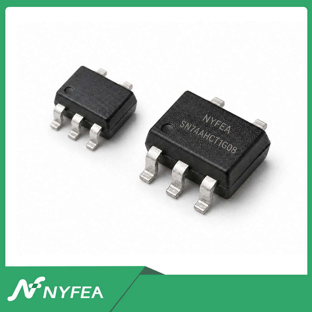
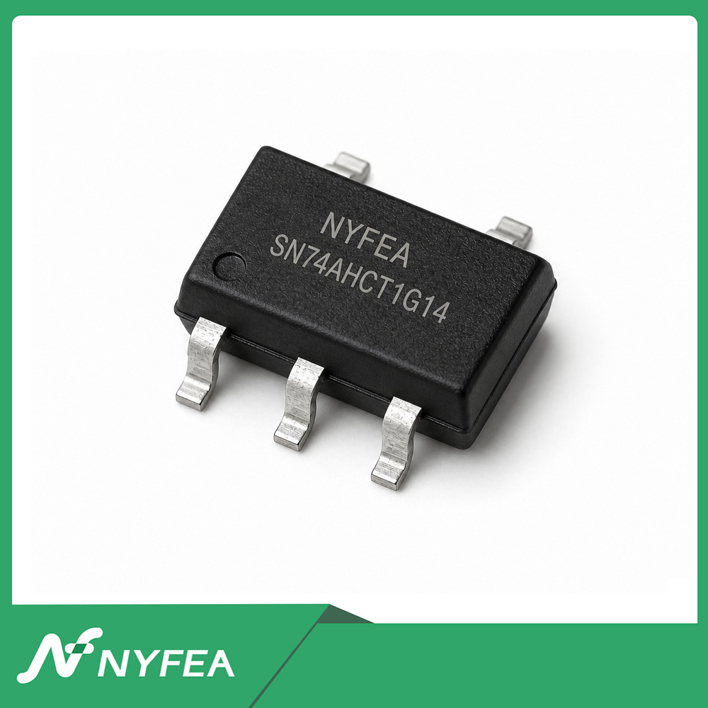
SN74AHCT1G14
±32 mA at VCC = 5.0 V under stated DC conditions,Single Schmitt-trigger inverter, Y = NOT A
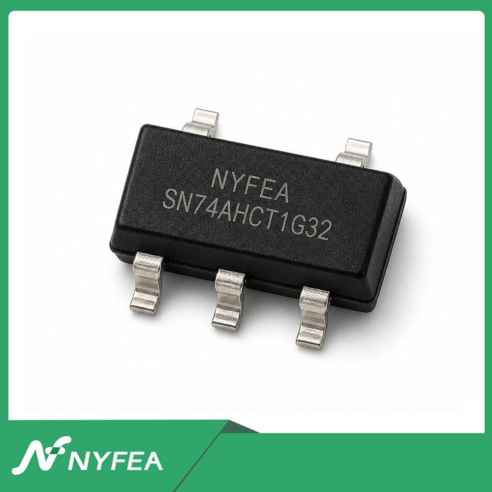
SN74AHCT1G32
This device implements Y = A + B in positive logic. A HIGH level on either input drives the output HIGH; both inputs must be LOW for a LOW output.
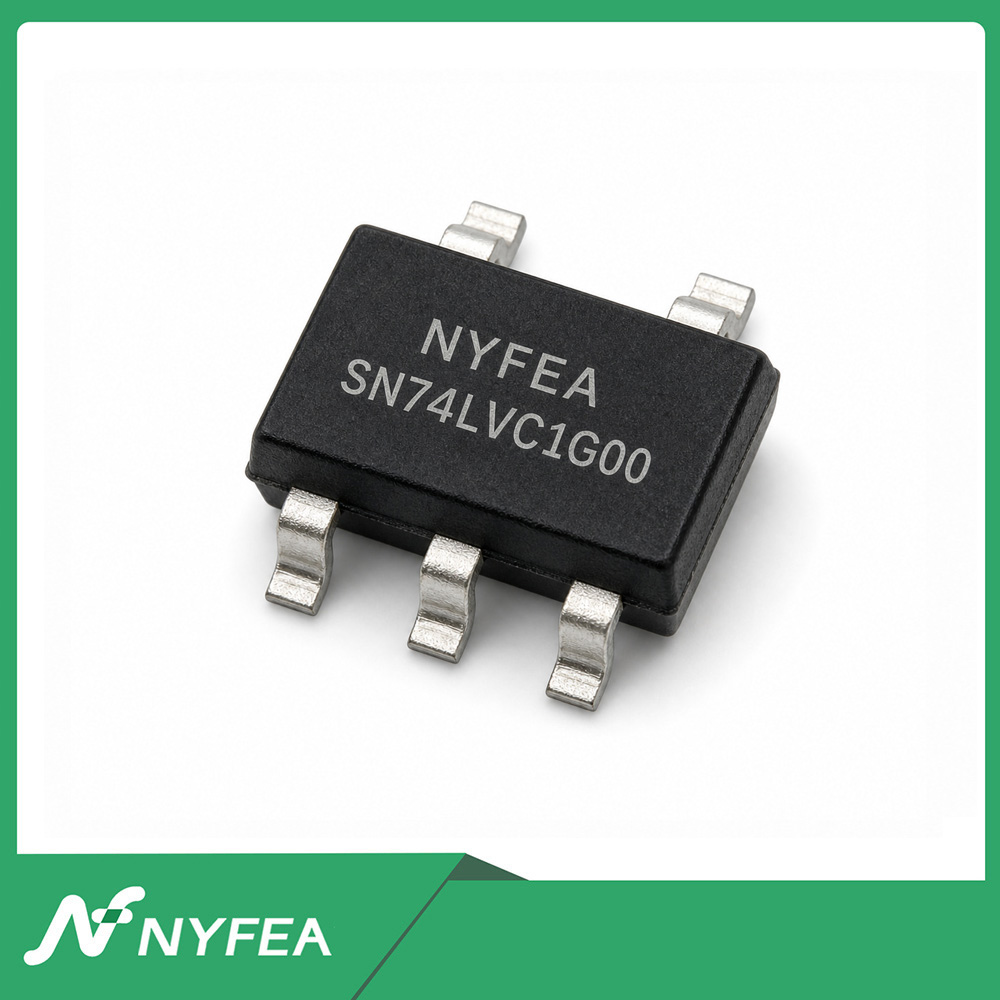
SN74LVC1G00
Single 2-input positive-NAND gate specified for 1.65 V to 5.5 V operation. It accepts input voltages up to 5.5 V
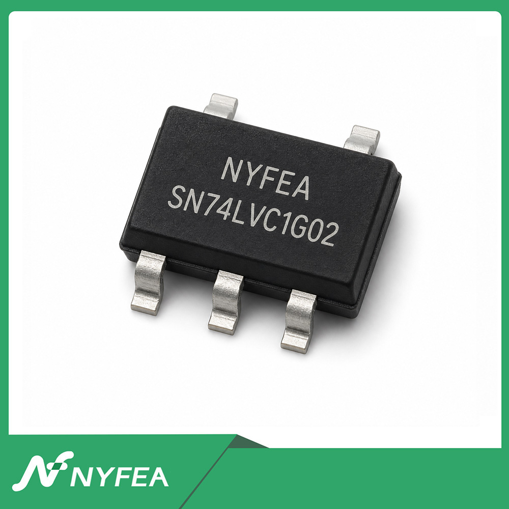
SN74LVC1G02
Single 2-input positive-NOR gate specified for 1.65 V to 5.5 V operation. Its inputs accept signals from 0 V to 5.5 V
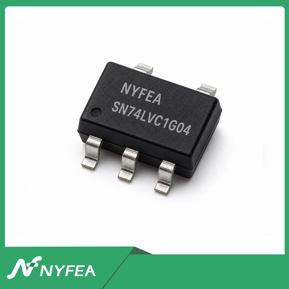
SN74LVC1G04
VCC is 1.65 V to 5.5 V for operation. VIH and VIL limits change with VCC; use the complete threshold table.
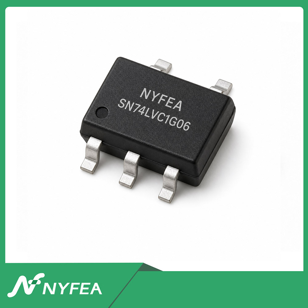
SN74LVC1G06
Single inverting buffer and driver with an open-drain output, specified for 1.65 V to 5.5 V VCC operation. Input A and open-drain output Y accept 0 V to 5.5 V,
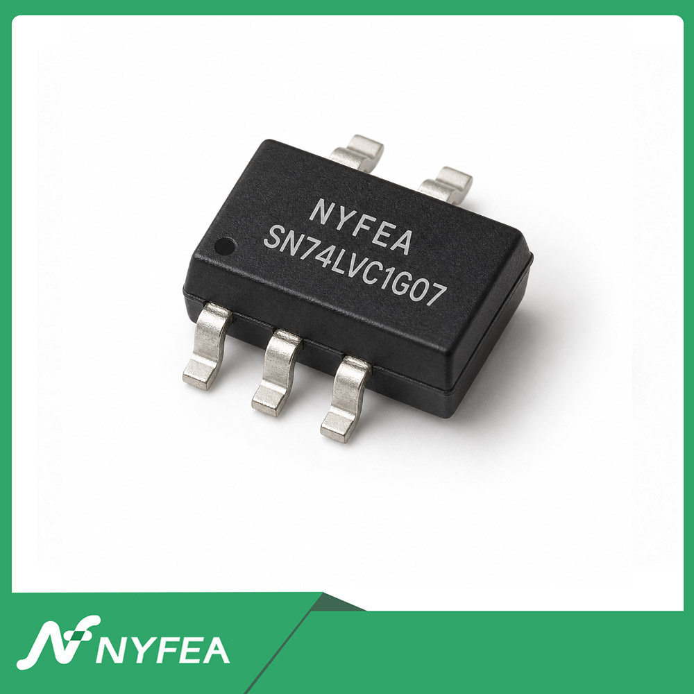
SN74LVC1G07
Combines a non-inverting input stage with an open-drain NMOS output. It can pull a shared node LOW but cannot actively drive it HIGH
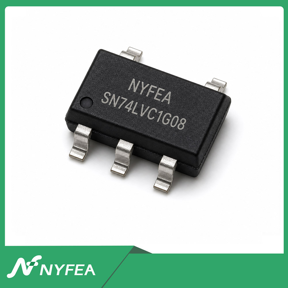
SN74LVC1G08
Single 2-input positive-AND gate specified for 1.65 V to 5.5 V operation. It accepts input voltages up to 5.5 V,
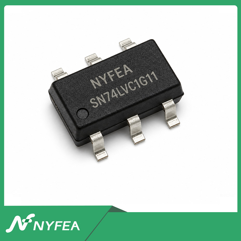
SN74LVC1G11
Integrates one 3-input positive-AND gate. Its output is HIGH only when A, B and C are simultaneously HIGH
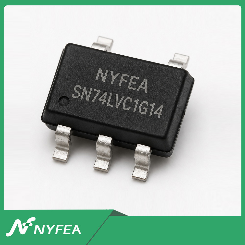
SN74LVC1G14
A single-gate inverter for 1.65 V to 5.5 V systems. Separate rising and falling input thresholds provide hysteresis
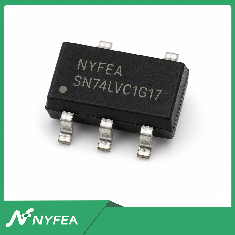
SN74LVC1G17
The values on this page are taken from the supplied SN74LVC1G17 Rev A.1 product specification. Before production release
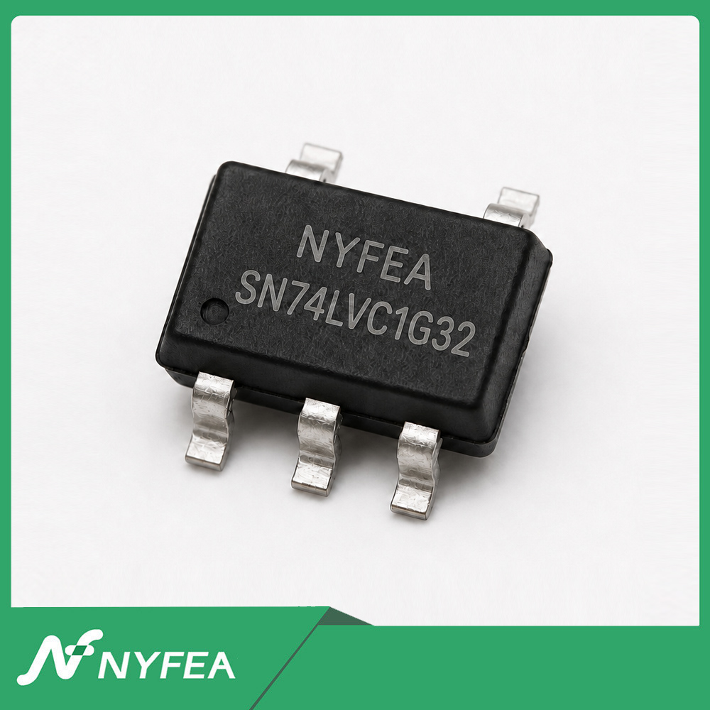
SN74LVC1G32
Hold every unused input at VCC or GND. The 0 V to 5.5 V input range does not imply that the push-pull output can tolerate an external overvoltage while the device is powered
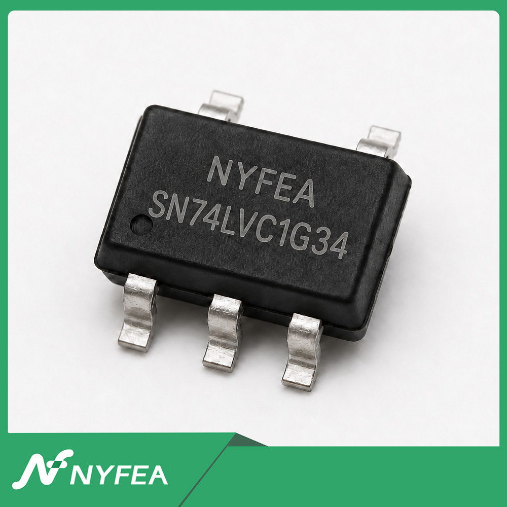
SN74LVC1G34
The values on this page are taken from the supplied SN74LVC1G34 Rev A.1 product specification. Before production release, verify the current controlled specification
SN74LVC1G34
The values on this page are taken from the supplied SN74LVC1G34 Rev A.1 product specification. Before production release, verify the current controlled specification
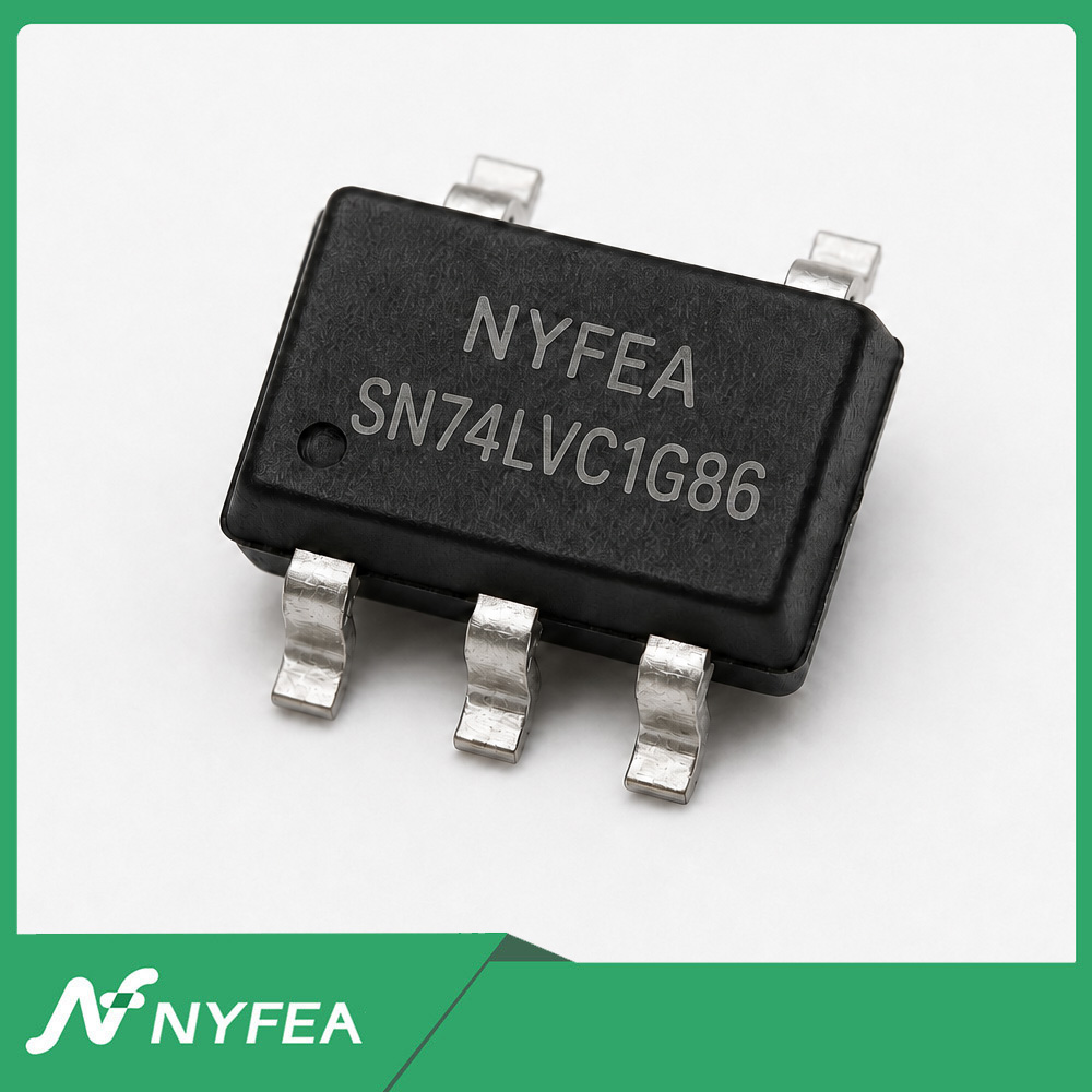
SN74LVC1G86
The values on this page are taken from the supplied SN74LVC1G34 Rev A.1 product specification. Before production release, verify the current controlled specification
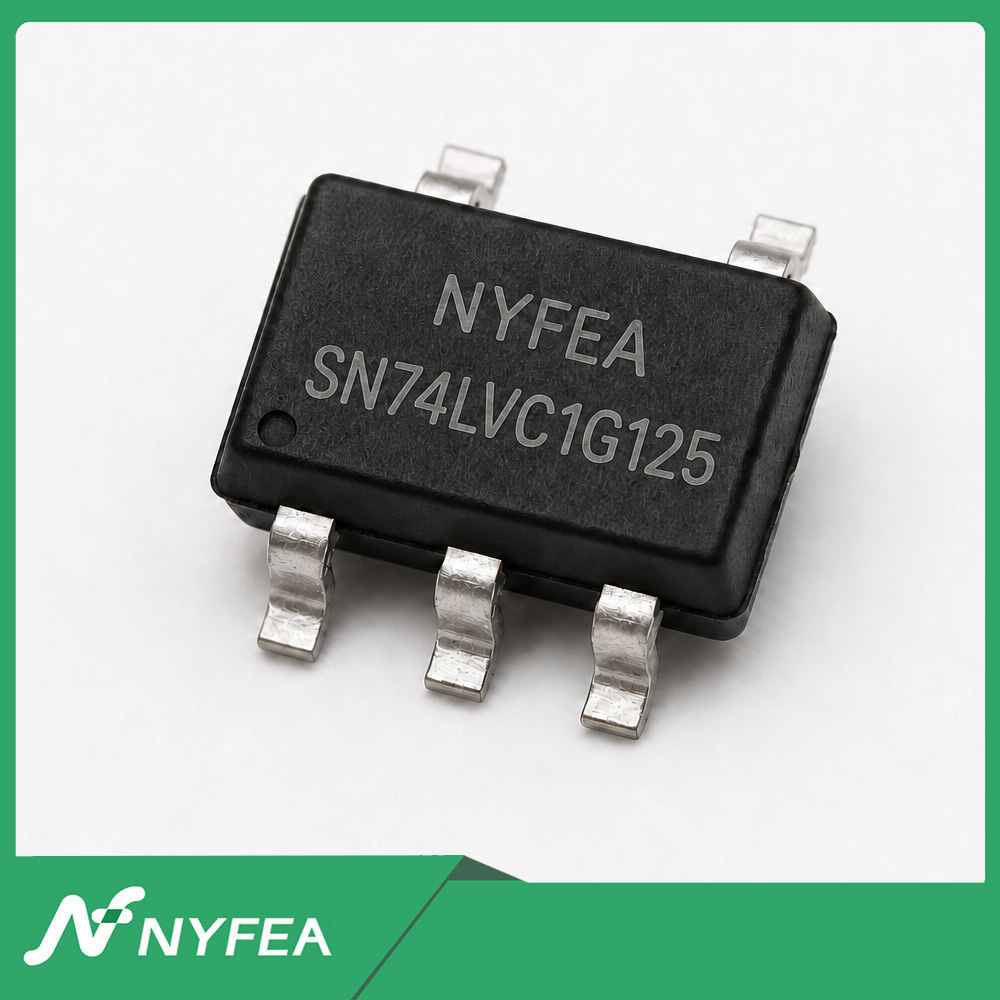
SN74LVC1G125
SN74LVC1G125 is a single non-inverting line driver specified for operation from 1.65 V to 5.5 V. With active-LOW /OE asserted, Y follows A; driving /OE HIGH places Y in the high-impedance state
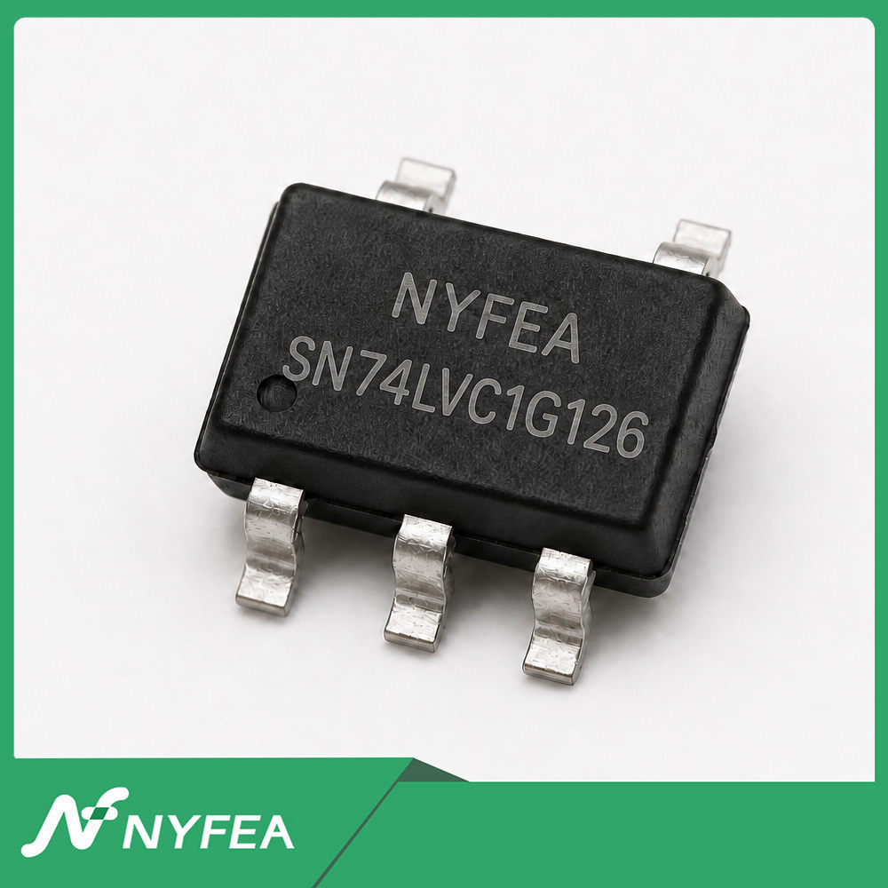
SN74LVC1G126
A compact noninverting line driver for 1.65 V to 5.5 V systems. When OE is HIGH, Y follows A; when OE is LOW, Y enters the high-impedance state.
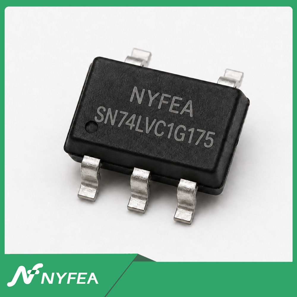
SN74LVC1G175
A compact noninverting line driver for 1.65 V to 5.5 V systems. When OE is HIGH, Y follows A; when OE is LOW, Y enters the high-impedance state.
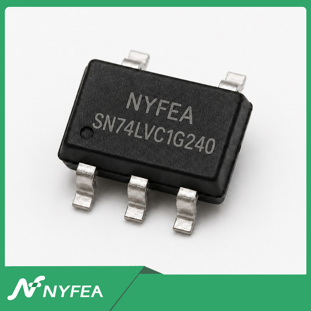
sn74lvc1g240
A compact single-channel line driver for 1.65 V to 5.5 V systems. When OE is LOW, Y is the inverse of A.
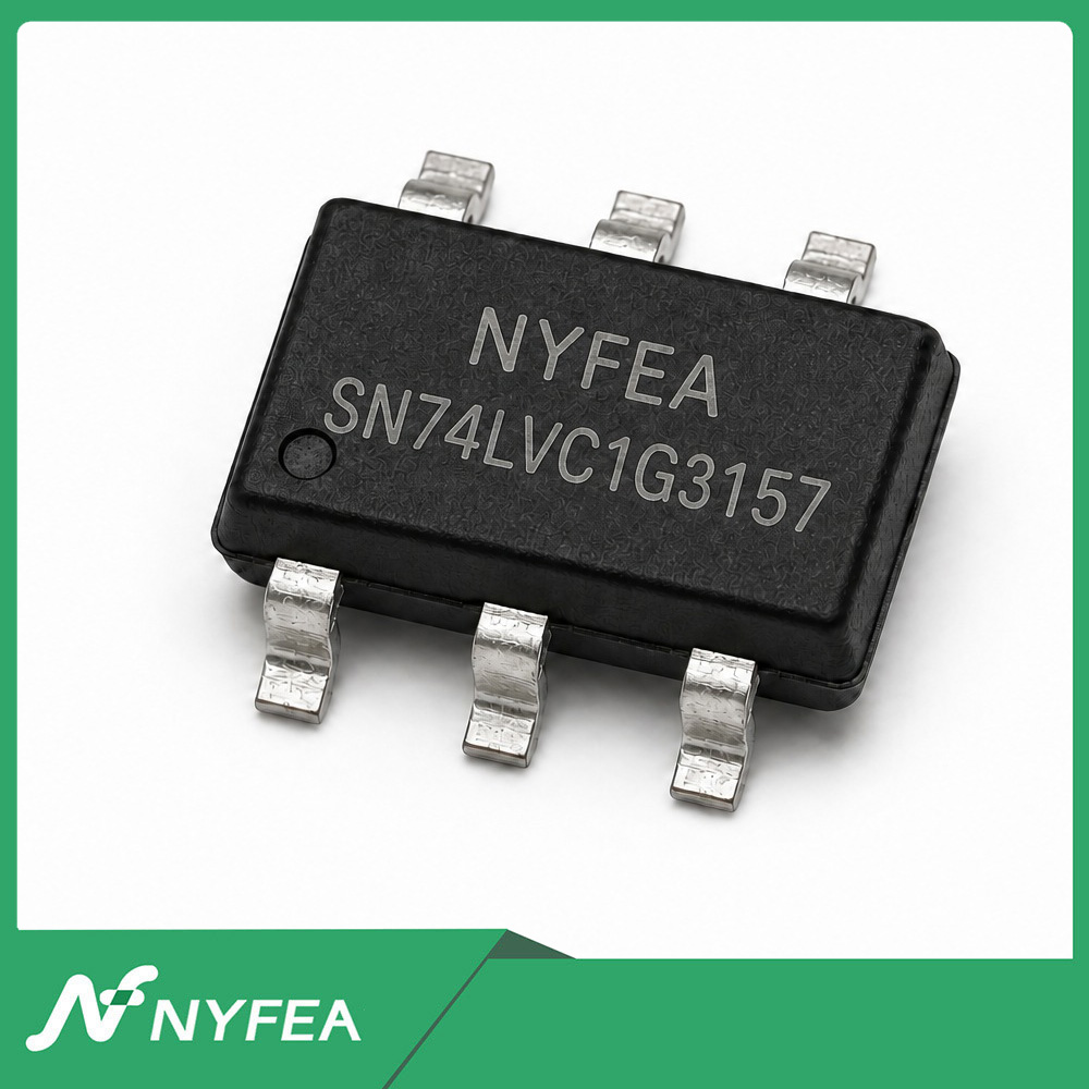
SN74LVC1G3157
A single-pole double-throw switch for routing analog or digital signals from 0 V to V+. It combines 4.5 Ω typical on-resistance at 5 V, 300 MHz typical bandwidth and 1.8 V to 5.5 V supply operation.
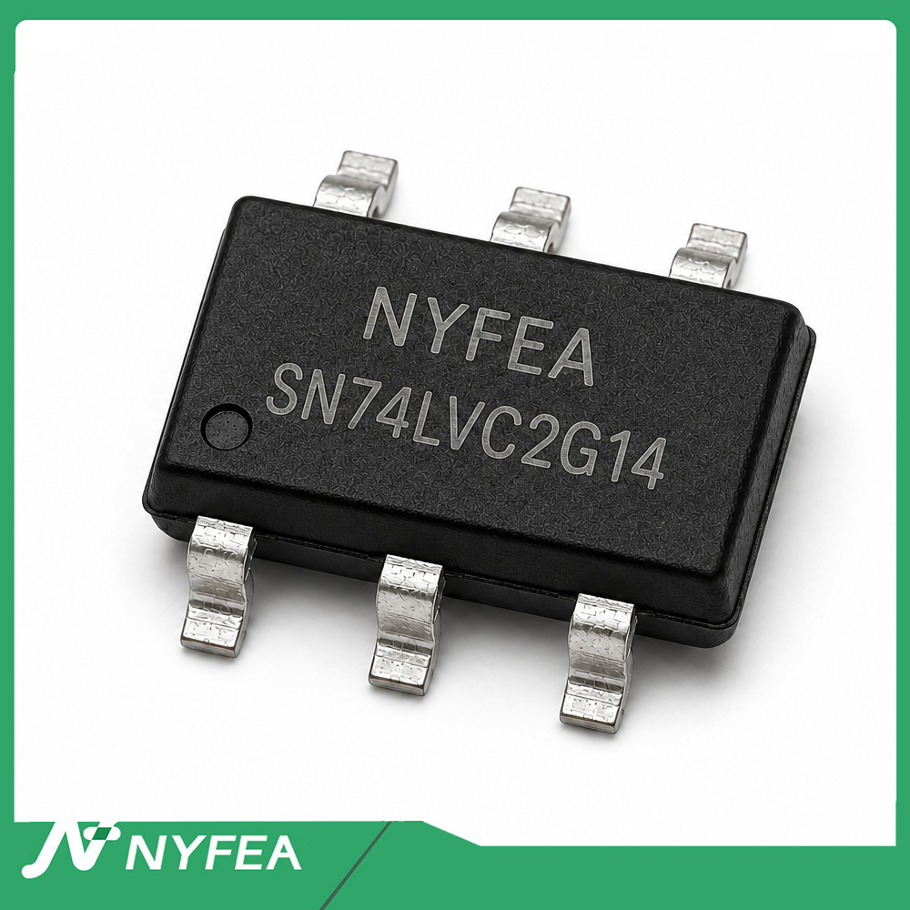
sn74lvc2g14
This device has two inverting Schmitt-trigger channels with actively driven outputs. It is not a plain-threshold inverter, open-drain output, tri-state driver or analog comparator.
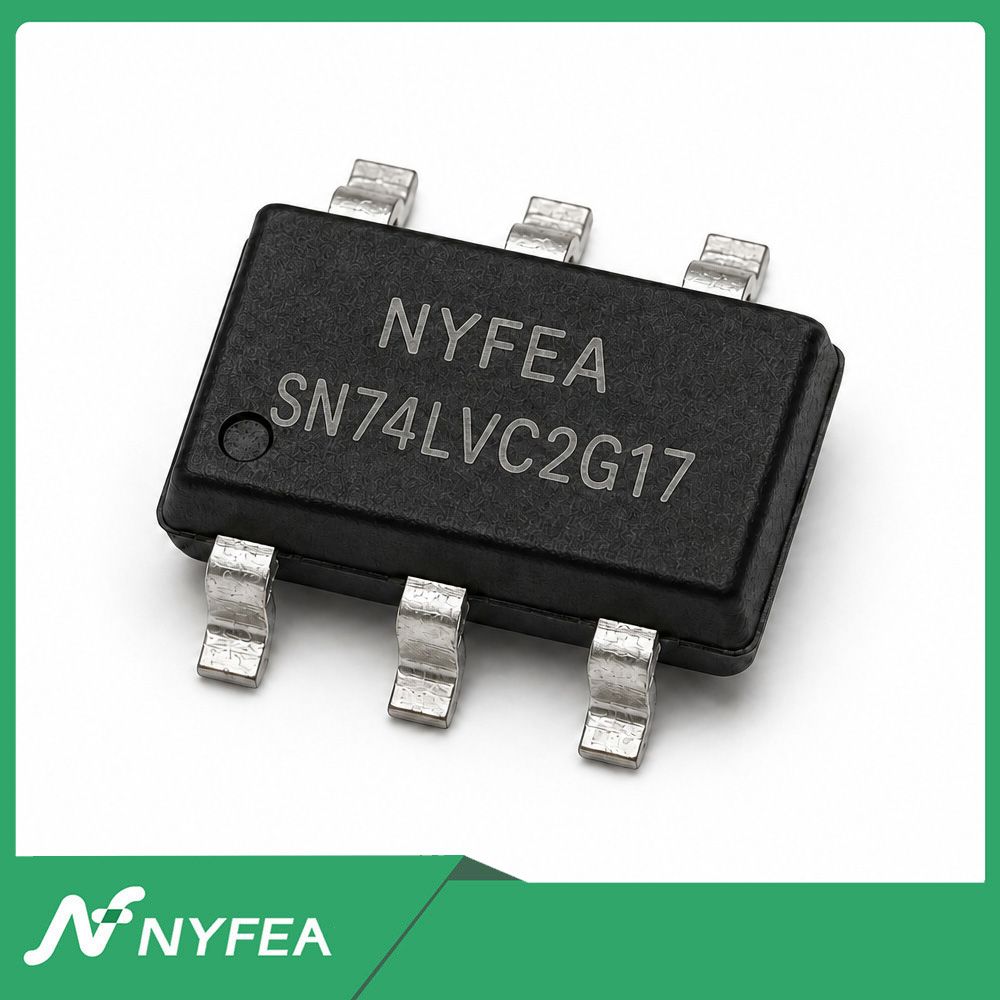
sn74lvc2g17
Values on this page are derived from the supplied SN74LVC2G17 Rev A.1 product specification
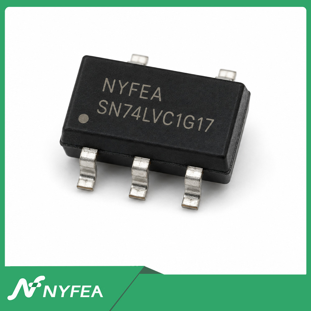
SN74LVC2G34
Two independent non-inverting buffer gates for 1.65 V to 5.5 V systems, combining low static power with high output drive and 5.5 V-tolerant inputs.