
SN74AHCT1G32 Single 2-Input Positive-OR Gate
NYFEA SN74AHCT1G32 is a single 2-input positive-OR gate for a 2.0 V to 5.5 V supply. It provides TTL-compatible inputs, Ioff partial-power-down support and a push-pull output in a compact green SOT23-5 package.
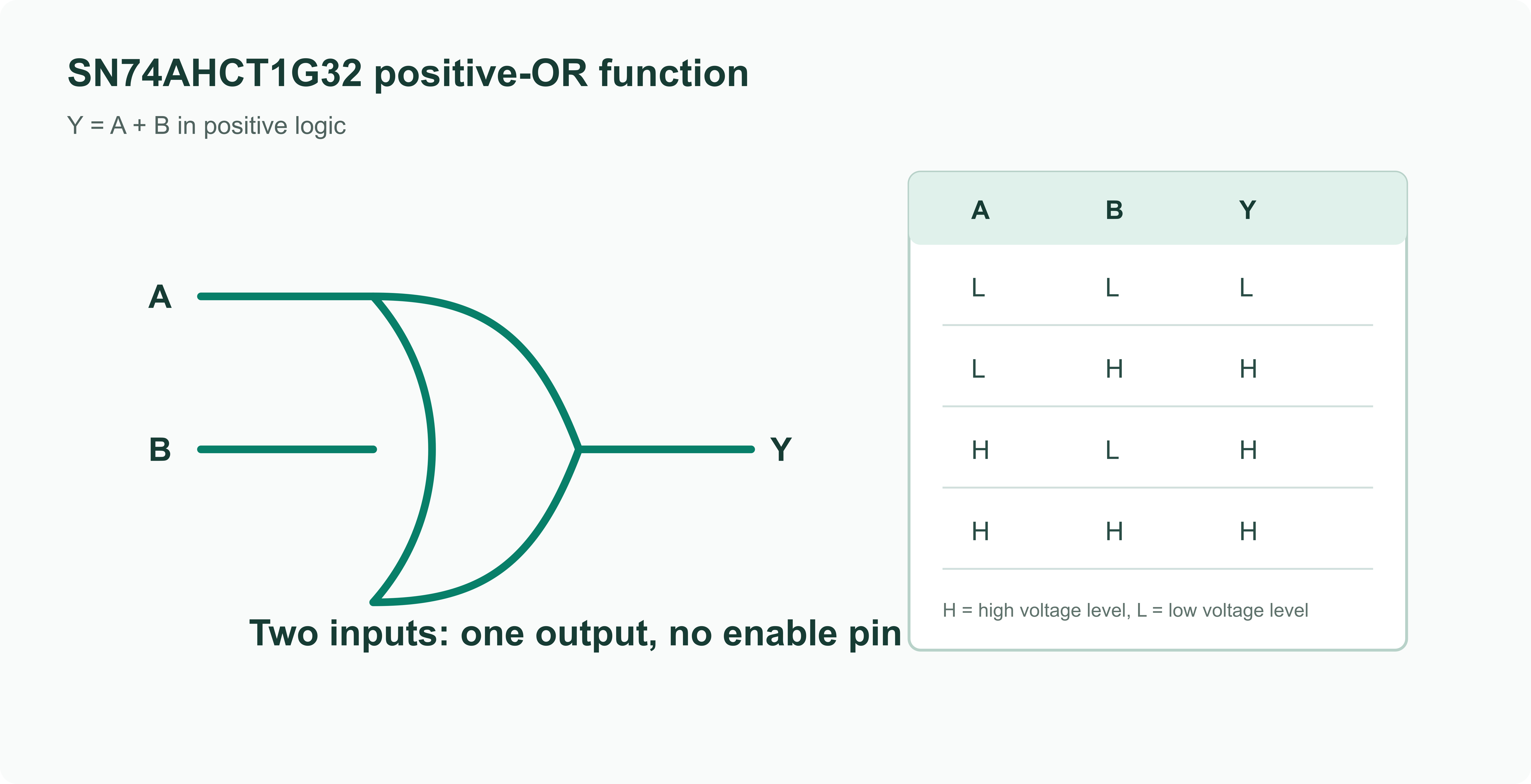
Product scope: This device implements Y = A + B in positive logic. A HIGH level on either input drives the output HIGH; both inputs must be LOW for a LOW output. It is a logic gate, not an analog adder, Schmitt trigger, level translator or tri-state buffer.
Use the current controlled PDF for logic thresholds, output loading, switching conditions, package tolerances, tape orientation and production-release decisions.
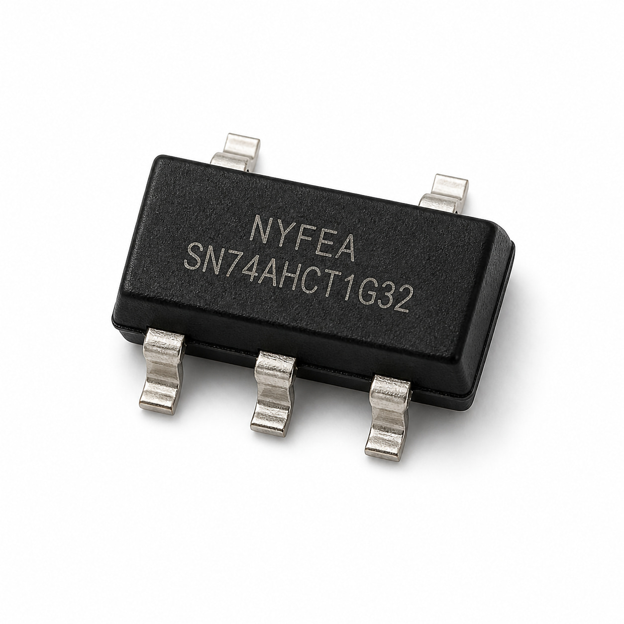
Product Overview and Selection Scope
SN74AHCT1G32 integrates one 2-input positive-OR gate. The Boolean function is Y = A + B, so the output is HIGH whenever A or B is HIGH. The device is specified for a 2.0 V to 5.5 V supply, 0 V to 5.5 V input and output operating ranges, and -40 °C to +125 °C ambient operation.
Signal role
Two CMOS/TTL-compatible inputs, A and B, feed one push-pull output Y. There is no enable or output-control pin.
Voltage domain
Recommended VCC is 2.0 V to 5.5 V. VIH and VIL limits vary with VCC; use the DC table rather than a single nominal threshold.
Power-down behavior
Ioff is specified with VCC = 0 V and VI or VO = 5.5 V to limit damaging current backflow through the powered-down device path.
Package
Green SOT23-5, ordering code SN74AHCT1G32DBVR, B32S top marking, MSL 3 and tape-and-reel packing of 3,000 units.
Selection boundary: The PDF does not define analog summing accuracy, hysteresis, tri-state operation, fail-safe input behavior, data-converter performance or end-product qualification. Validate the complete signal chain and system environment.
Logic Function, Truth Table and Pin Assignment
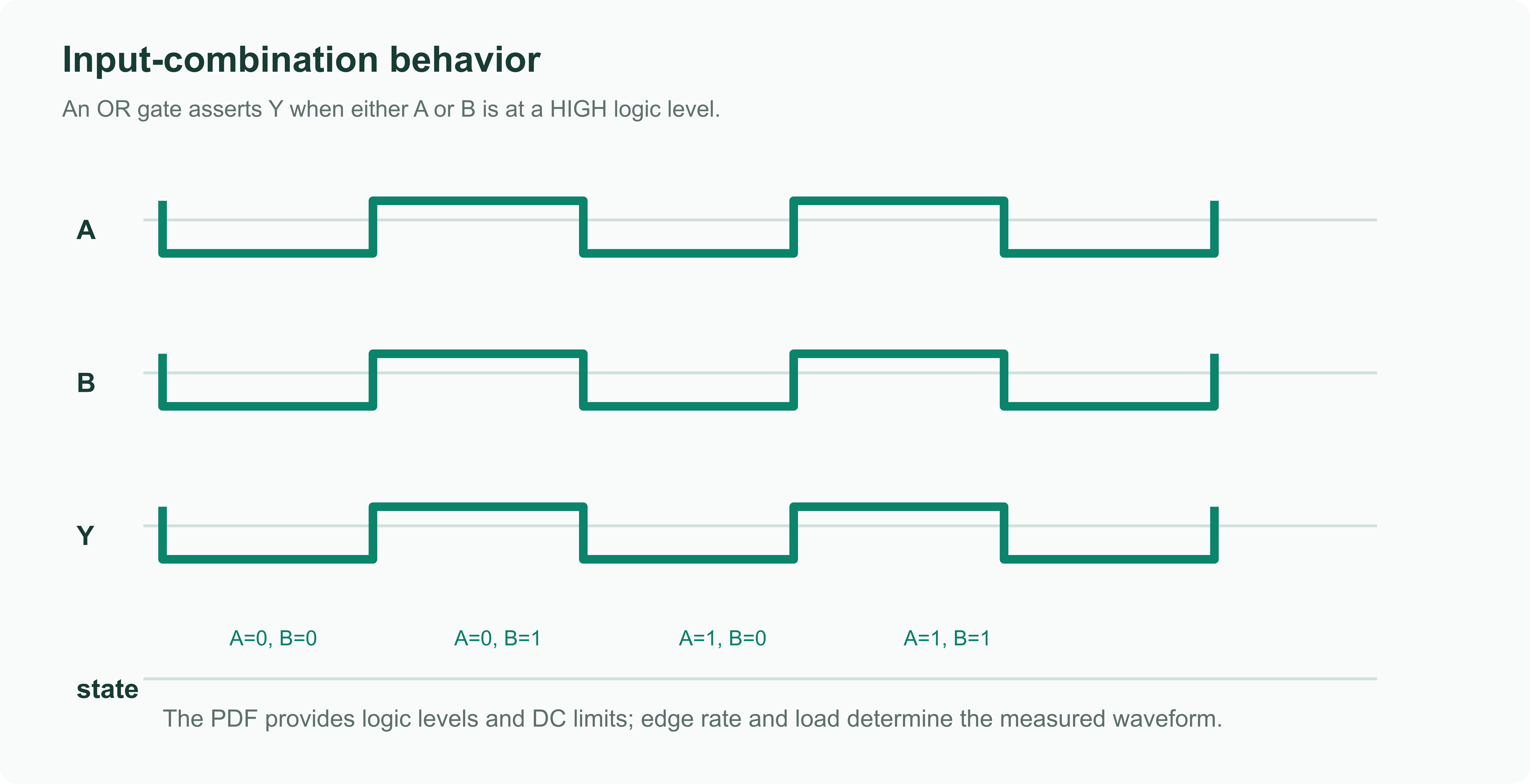
In positive logic, Y = A + B. The output is LOW only for A = LOW and B = LOW. The function table below is the direct logic definition; the measured transition waveform additionally depends on input edge rate, load capacitance and supply voltage.
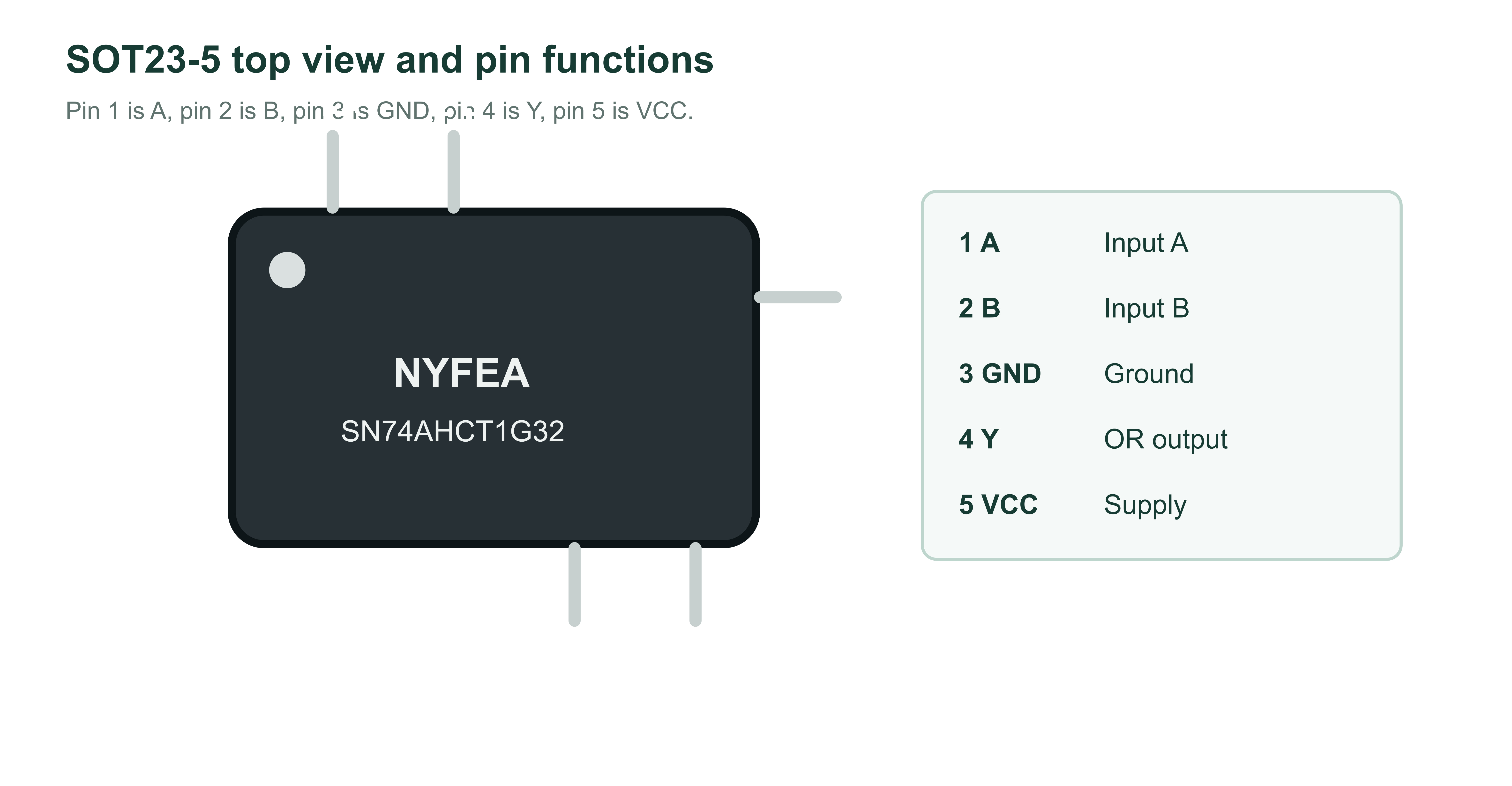
| Pin | Name | Type | Function | Engineering note |
|---|---|---|---|---|
| 1 | A | Input | First positive-logic input | Hold at VCC or GND when unused. |
| 2 | B | Input | Second positive-logic input | Hold at VCC or GND when unused. |
| 3 | GND | Power | Ground | Use a short return to the local bypass capacitor. |
| 4 | Y | Output | Push-pull OR output | Verify VOH/VOL for the receiving load. |
| 5 | VCC | Power | Supply | Place local decoupling near pins 5 and 3. |
Ordering Code and Package Selection
| Product | Ordering number | Temperature range | Package | Marking | MSL | Packing |
|---|---|---|---|---|---|---|
| SN74AHCT1G32 | SN74AHCT1G32DBVR | -40 °C to +125 °C | SOT23-5 | B32S | MSL 3 | Tape and reel, 3,000 units |
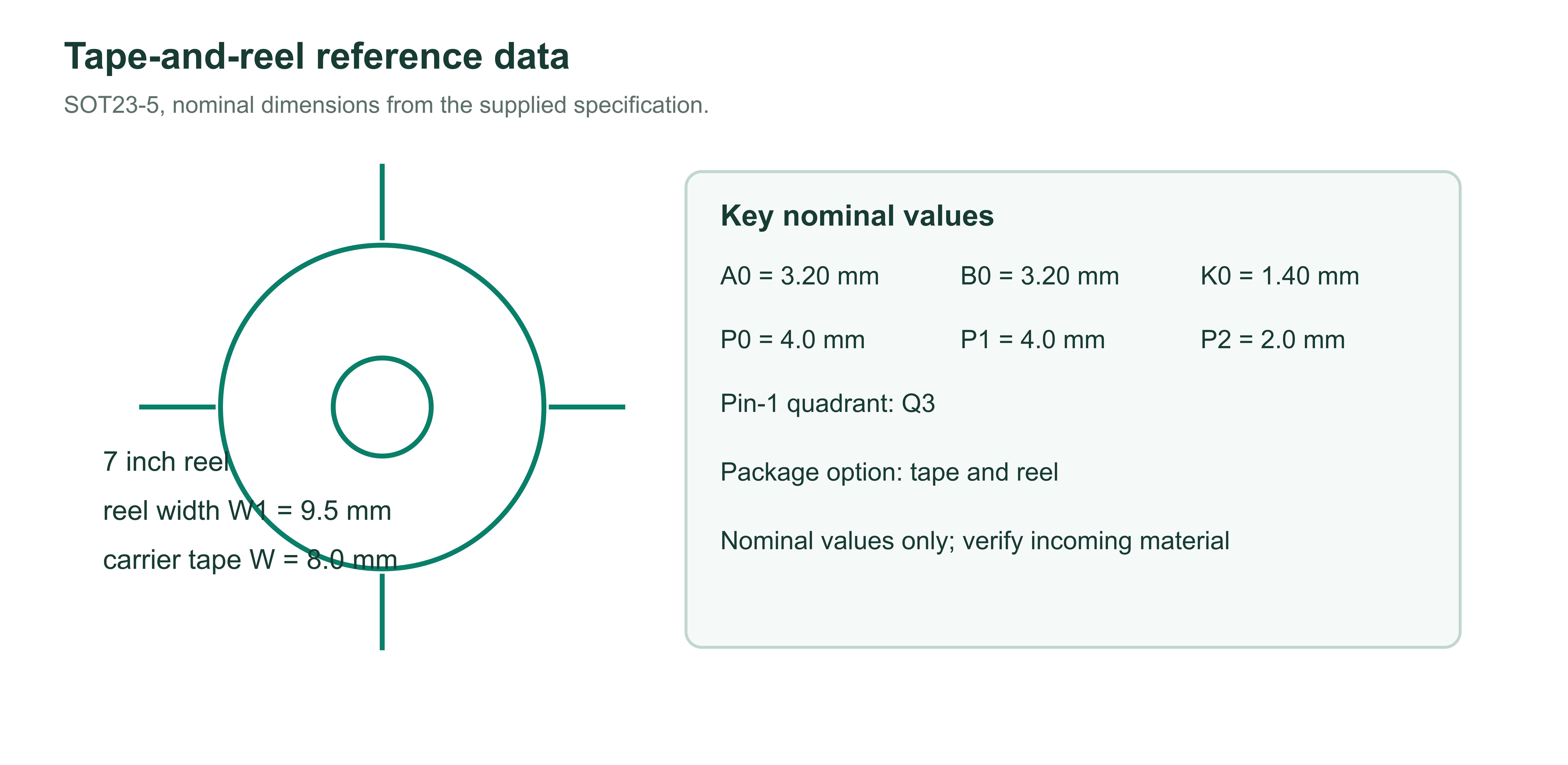
The specification notes that additional lot, date, vendor, logo or environmental markings may appear. Confirm the ordering code, top marking, reel orientation and current document revision at receiving inspection.
Recommended Operating Conditions and Absolute Limits
Recommended operating conditions define the functional design range. Absolute maximum ratings are stress limits and do not imply functional operation or long-term reliability.
| Parameter | Symbol | Condition | Minimum | Maximum | Unit |
|---|---|---|---|---|---|
| Supply voltage | VCC | Operating | 2.0 | 5.5 | V |
| High-level input voltage | VIH | VCC = 2.0 / 3.3 / 4.5 to 5.5 V | 1.0 / 1.5 / 2.0 | - | V |
| Low-level input voltage | VIL | VCC = 2.0 / 3.3 / 4.5 to 5.5 V | - | 0.3 / 0.55 / 0.8 | V |
| Input voltage | VI | Operating | 0 | 5.5 | V |
| Output voltage | VO | Operating | 0 | VCC | V |
| Input transition rate | Δt/Δv | VCC = 2.0 V to 5.5 V | - | 5 | ns/V |
| Ambient temperature | TA | Operating | -40 | 125 | °C |
Absolute maximum and handling limits
| Parameter | Condition | Minimum | Maximum | Unit |
|---|---|---|---|---|
| Supply voltage | VCC | -0.5 | 6.5 | V |
| Input voltage | VI | -0.5 | 6.5 | V |
| Output voltage, high-impedance or power-off | VO | -0.5 | 6.5 | V |
| Output voltage, HIGH or LOW state | VO | -0.5 | VCC + 0.5 | V |
| Input clamp current | IIK, VI < 0 V | - | -50 | mA |
| Output clamp current | IOK, VO < 0 V | - | -50 | mA |
| Continuous output current | IO | ±50 | mA | |
| Continuous VCC or GND current | - | ±100 | mA | |
| Junction temperature | TJ | -65 | 150 | °C |
| Storage temperature | Tstg | -65 | 150 | °C |
DC Characteristics and Logic Levels
Unless otherwise noted, full-range limits apply from -40 °C to +125 °C. Typical values are characterized at +25 °C; they are not guaranteed limits.
| Parameter | Test condition | VCC | Temperature | Minimum | Typical | Maximum | Unit |
|---|---|---|---|---|---|---|---|
| VIH high-level input | Guaranteed input level | 2.0 V | Full | 1.0 | - | - | V |
| VIH high-level input | Guaranteed input level | 3.3 V | Full | 1.5 | - | - | V |
| VIH high-level input | Guaranteed input level | 4.5 V to 5.5 V | Full | 2.0 | - | - | V |
| VIL low-level input | Guaranteed input level | 2.0 V | Full | - | - | 0.3 | V |
| VIL low-level input | Guaranteed input level | 3.3 V | Full | - | - | 0.55 | V |
| VIL low-level input | Guaranteed input level | 4.5 V to 5.5 V | Full | - | - | 0.8 | V |
Output levels, leakage and supply current
| Parameter | Test condition | VCC | Temperature | Minimum / typical / maximum | Unit |
|---|---|---|---|---|---|
| VOH | IOH = -100 µA | 2.0 V to 5.5 V | Full | Minimum VCC - 0.1 V | V |
| VOH | IOH = -8 / -24 / -32 mA | 2.0 / 3.3 / 4.5 / 5.0 / 5.5 V | Full | Minimum 1.6 / 2.5 / 3.8 / 4.2 / 4.8 V | V |
| VOL | IOL = 100 µA | 2.0 V to 5.5 V | Full | Maximum 0.1 V | V |
| VOL | IOL = 8 / 24 / 32 mA | 2.0 / 3.3 / 4.5 / 5.0 / 5.5 V | Full | Maximum 0.45 / 0.55 / 0.55 / 0.50 / 0.45 V | V |
| II | A or B input at 5.5 V or GND | 0 V to 5.5 V | +25 °C / Full | Typical ±0.1 µA / maximum ±5 µA | µA |
| Ioff | VI or VO = 5.5 V | 0 V | +25 °C / Full | Typical ±0.1 µA / maximum ±10 µA | µA |
| ICC | VI = 5.5 V or GND, IO = 0 | 2.0 V to 5.5 V | +25 °C / Full | Typical 0.1 µA / maximum 10 µA | µA |
| ICCT | One input at 3.4 V, other at VCC or GND | 5.5 V | Full | Maximum 500 µA | µA |
| Ci | VCC = 0 V, f = 10 MHz | 0 V | +25 °C | Typical 6 | pF |
AC Switching and Test Conditions
The PDF lists propagation-delay and power-dissipation-capacitance values as typical values at +25 °C. It states that these parameters are ensured by design and/or characterization and are not tested in production; no guaranteed maximum propagation delay is listed.
| Parameter | VCC | Load | Temperature | Typical | Guaranteed maximum | Unit |
|---|---|---|---|---|---|---|
| Propagation delay, tpd | 2.0 V ±0.2 V | CL = 30 pF, RL = 500 Ω | +25 °C | 3.8 | Not specified | ns |
| Propagation delay, tpd | 3.3 V ±0.3 V | CL = 50 pF, RL = 500 Ω | +25 °C | 2.6 | Not specified | ns |
| Propagation delay, tpd | 5.0 V ±0.5 V | CL = 50 pF, RL = 500 Ω | +25 °C | 2.8 | Not specified | ns |
| Power-dissipation capacitance, Cpd | 5 V | f = 10 MHz | +25 °C | 25 | Not specified | pF |
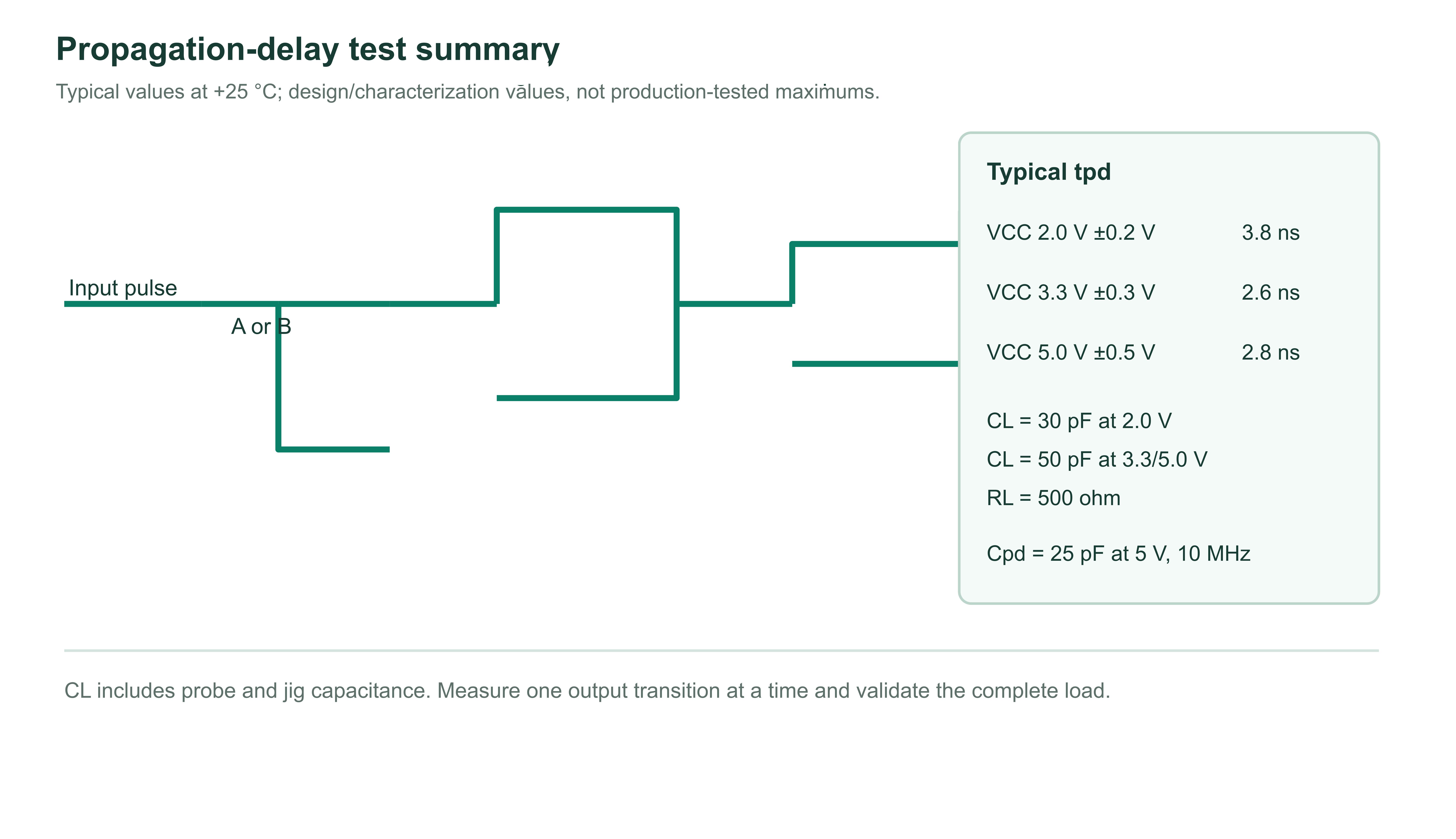
Applicability note: The PDF also shows generic enable/disable waveform templates, but SN74AHCT1G32 has no enable pin. Do not infer tri-state or output-enable behavior from those generic diagrams.
Power Integrity, Input Handling and PCB Layout
Use the layout below as an application-design checklist, not as a guaranteed reference circuit. The controlled PDF defines the electrical limits; the complete board power-distribution network and receiving device determine the final implementation.
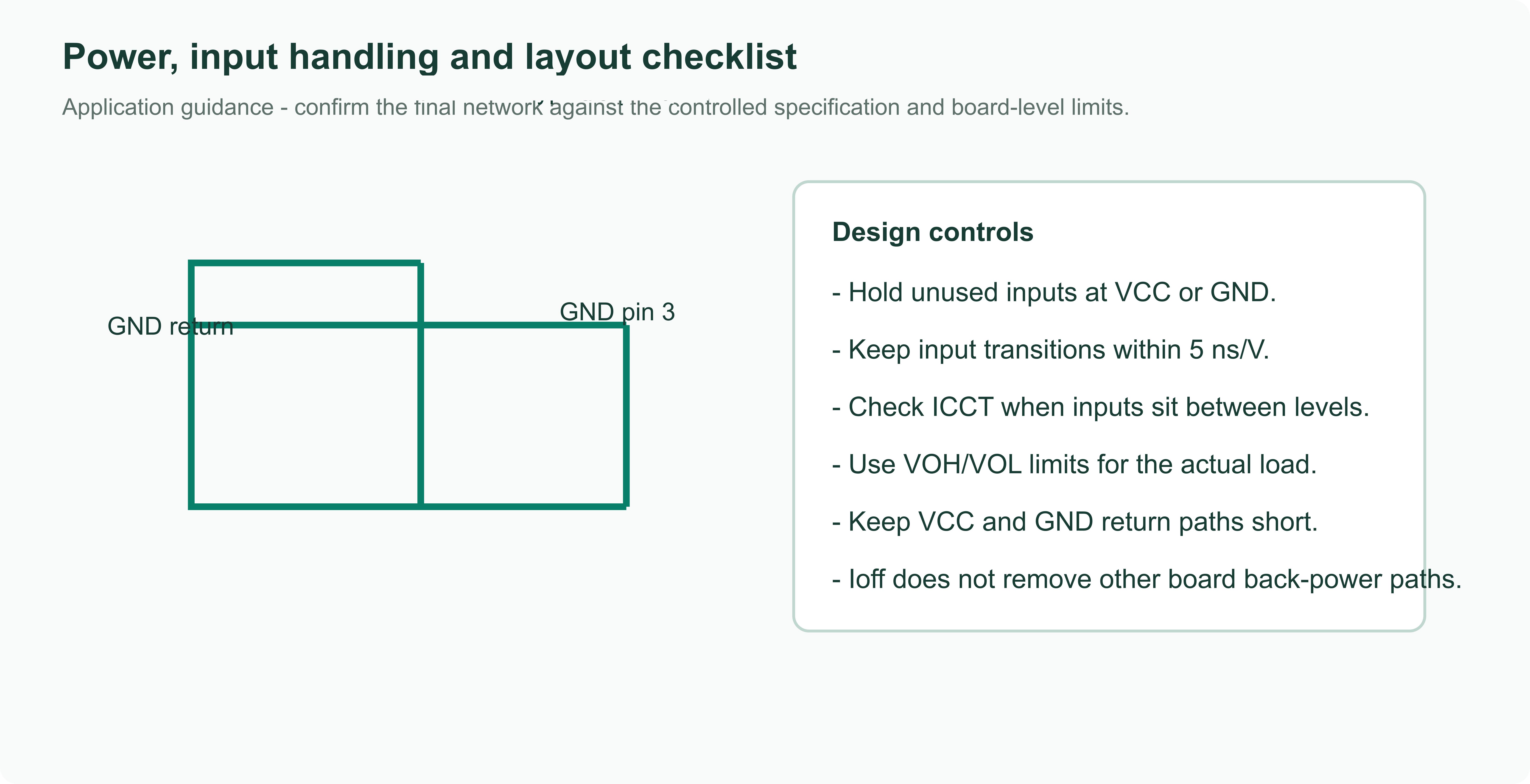
- Do not leave A or B floating: connect unused inputs to VCC or GND.
- Respect input transition limits: the recommended operating table lists a maximum Δt/Δv of 5 ns/V.
- Budget transition current: an input at 3.4 V under the ICCT test condition can increase supply current to the listed 500 µA maximum.
- Check output levels: ±32 mA is tied to the stated 5.0 V DC output conditions; it is not a general-purpose power-drive rating.
- Prevent contention: Y is a push-pull output with no enable pin; do not tie it to another actively driven output.
- Validate partial power-down: Ioff characterizes the device path, while other board components can still create back-power paths.
SOT23-5 Package, Land Pattern and Tape-and-Reel Data
The single listed package is green SOT23-5. Dimensions below reproduce the source drawing; PCB-library release must still use the complete controlled PDF and the assembler's land-pattern rules.
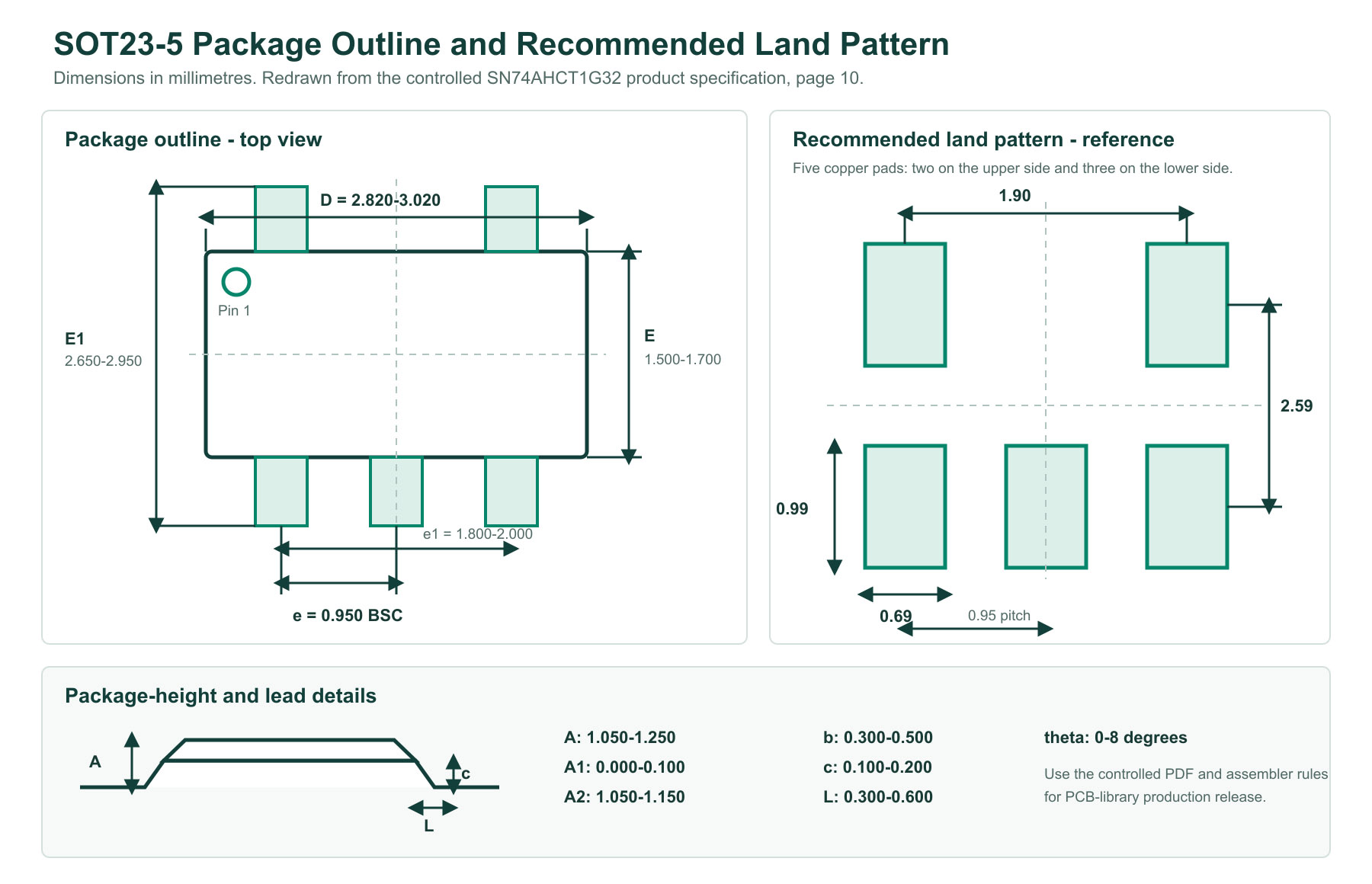
| Symbol | Minimum | Maximum | Unit | Meaning |
|---|---|---|---|---|
| A | 1.050 | 1.250 | mm | Overall height |
| A1 | 0.000 | 0.100 | mm | Seating offset |
| A2 | 1.050 | 1.150 | mm | Body height |
| b | 0.300 | 0.500 | mm | Lead width |
| c | 0.100 | 0.200 | mm | Lead thickness |
| D | 2.820 | 3.020 | mm | Body length |
| E | 1.500 | 1.700 | mm | Body width |
| E1 | 2.650 | 2.950 | mm | Overall lead span |
| e | 0.950 BSC | mm | Lead pitch | |
| e1 | 1.800 | 2.000 | mm | Outer lead pitch |
| L | 0.300 | 0.600 | mm | Lead length |
| θ | 0° | 8° | degree | Lead angle |
Application Guidance and Design Limitations
The Rev A.1 specification lists AV receivers, Blu-ray players and home theaters, digital picture frames, high-speed data acquisition and generation, personal navigation devices (GPS) and portable media players. These are possible use contexts, not end-product qualification statements.
 AV ReceiverCombine two local control conditions into one positive-logic enable or status signal. Validate VIH/VIL margins and the receiving load.
 Blu-ray Player and Home TheaterGate a reset, detect or control path. The gate does not process audio/video data and has no output-enable function.
 Digital Picture Frame (DPF)Merge display-ready status conditions before a local logic input. Confirm startup sequencing and standby current.
 High-Speed Data Acquisition and GenerationCombine trigger or qualification flags at the logic boundary. Propagation delay and load capacitance remain system-level timing terms.
 GPS and Portable Media PlayersUse for compact positive-logic condition combining after checking supply-domain compatibility, input transitions and power-down behavior.
SN74AHCT1G32 Engineering FAQs
What logic function does SN74AHCT1G32 implement?
It is one 2-input positive-OR gate. In positive logic, Y = A + B and the output is LOW only when both A and B are LOW.
What happens when only one input is HIGH?
Y is HIGH when A is HIGH and B is LOW, or when A is LOW and B is HIGH. It is also HIGH when both inputs are HIGH.
Does SN74AHCT1G32 provide hysteresis or an enable pin?
No. This PDF describes a standard positive-OR gate with two inputs and one push-pull output. It does not specify Schmitt hysteresis, tri-state control or output enable behavior.
What supply range is recommended?
VCC is specified from 2.0 V to 5.5 V under the recommended operating conditions.
What VIH and VIL limits should be used?
VIH minimum is 1.0 V at 2.0 V, 1.5 V at 3.3 V and 2.0 V at 4.5 V to 5.5 V. VIL maximum is 0.3 V, 0.55 V and 0.8 V respectively. Use the complete table for the full temperature range.
What does the 5 ns/V input-transition limit mean?
The recommended operating table lists a maximum input transition rate of 5 ns/V for VCC from 2.0 V to 5.5 V. Avoid leaving either input in an indeterminate region and consider ICCT in the power budget.
Are 3.8 ns, 2.6 ns and 2.8 ns guaranteed maximum delays?
No. They are typical values at +25 °C with the listed VCC, CL and RL conditions. The PDF does not list a guaranteed maximum propagation delay.
What does Ioff provide?
Ioff is specified with VCC = 0 V and VI or VO = 5.5 V to limit damaging current backflow through the powered-down device path. Check all other board-level back-power paths separately.
Which package and ordering code are listed?
The listed order code is SN74AHCT1G32DBVR in a green SOT23-5 package, with B32S top marking, MSL 3 and tape-and-reel packing of 3,000 units.
Do the listed applications establish product certification?
No. They identify possible use contexts only. Qualification, safety, EMC, reliability and production validation remain system responsibilities.
This page summarizes the SN74AHCT1G32 Rev A.1 product specification for component evaluation and engineering reference. It does not replace the complete controlled specification. Confirm the current revision, ordering code, marking, pin assignment, logic limits, absolute maximum ratings, DC and AC conditions, package tolerances, PCB layout, assembly process and qualification requirements before production release.
