
SN74LVC1G125 Single Bus Buffer Gate with 3-State Output
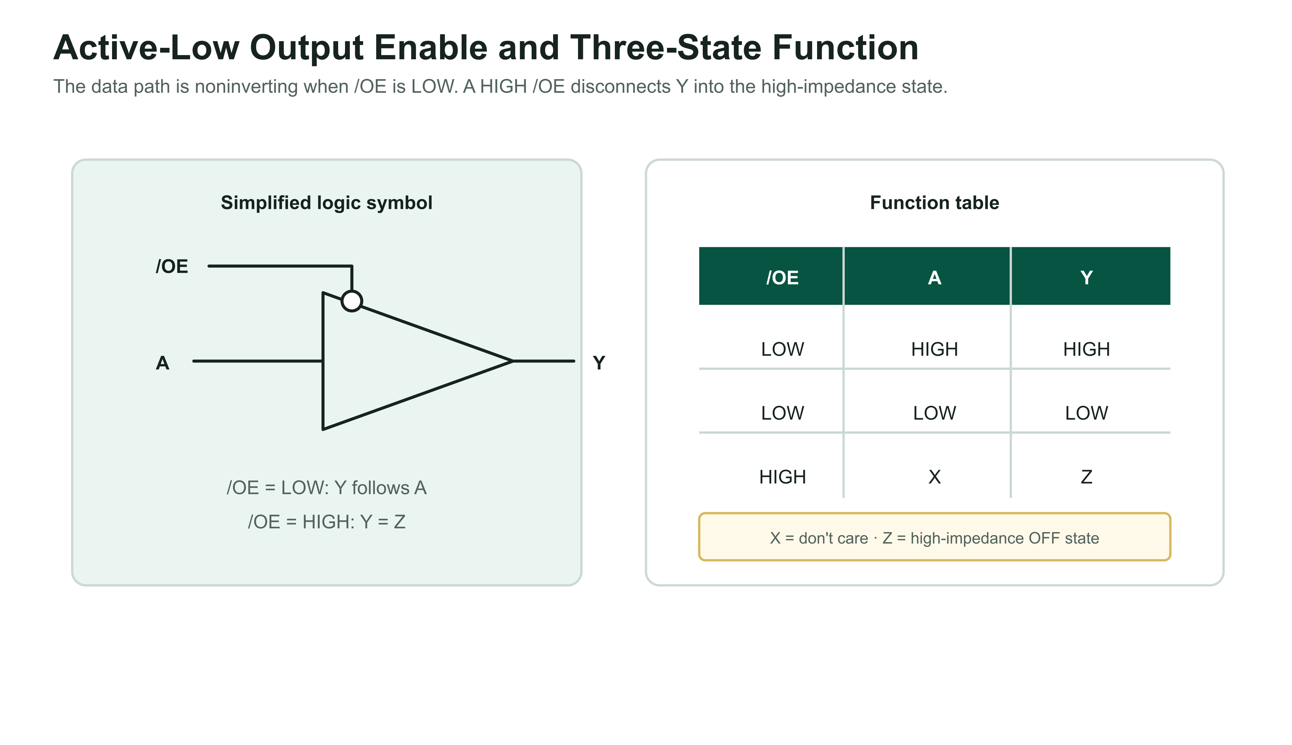
NYFEA SN74LVC1G125 is a single non-inverting line driver specified for operation from 1.65 V to 5.5 V. With active-LOW /OE asserted, Y follows A; driving /OE HIGH places Y in the high-impedance state. Ioff supports partial-power-down operation.
Product scope: This device is a unidirectional 3-state buffer. It is not an open-drain gate, analog switch, bidirectional bus transceiver, dual-supply level translator, or Schmitt-trigger input.
Use the current controlled PDF for thresholds, output loading, three-state timing, package tolerances, tape orientation and production-release decisions.

Product Overview and Selection Scope
SN74LVC1G125 combines a non-inverting data path with active-LOW output-enable control. When /OE is LOW, Y follows A as a push-pull logic output. Driving /OE HIGH places Y in the high-impedance state, enabling controlled isolation of a downstream load or connection to a shared node.
Data path
The enabled path is non-inverting. No data-storage, latching, clocking, or protocol function is provided.
Output isolation
/OE HIGH disables Y. Use break-before-make control when multiple push-pull drivers share one bus.
Power-down behavior
Ioff is specified with VCC = 0 V and limits current through the device during partial power-down. It does not eliminate external board-level back-power paths.
Package choice
SOT23-5 and SC70-5 share the pin assignment but use different markings, footprints and thermal impedances.
Selection boundary: An input range up to 5.5 V and a high-impedance output do not make this device a bidirectional level translator. Verify source levels, receiver VIH/VIL requirements, output swing, bus ownership, power sequencing, and off-state leakage at system level.
Logic Function, Three-State Control and Pin Assignment
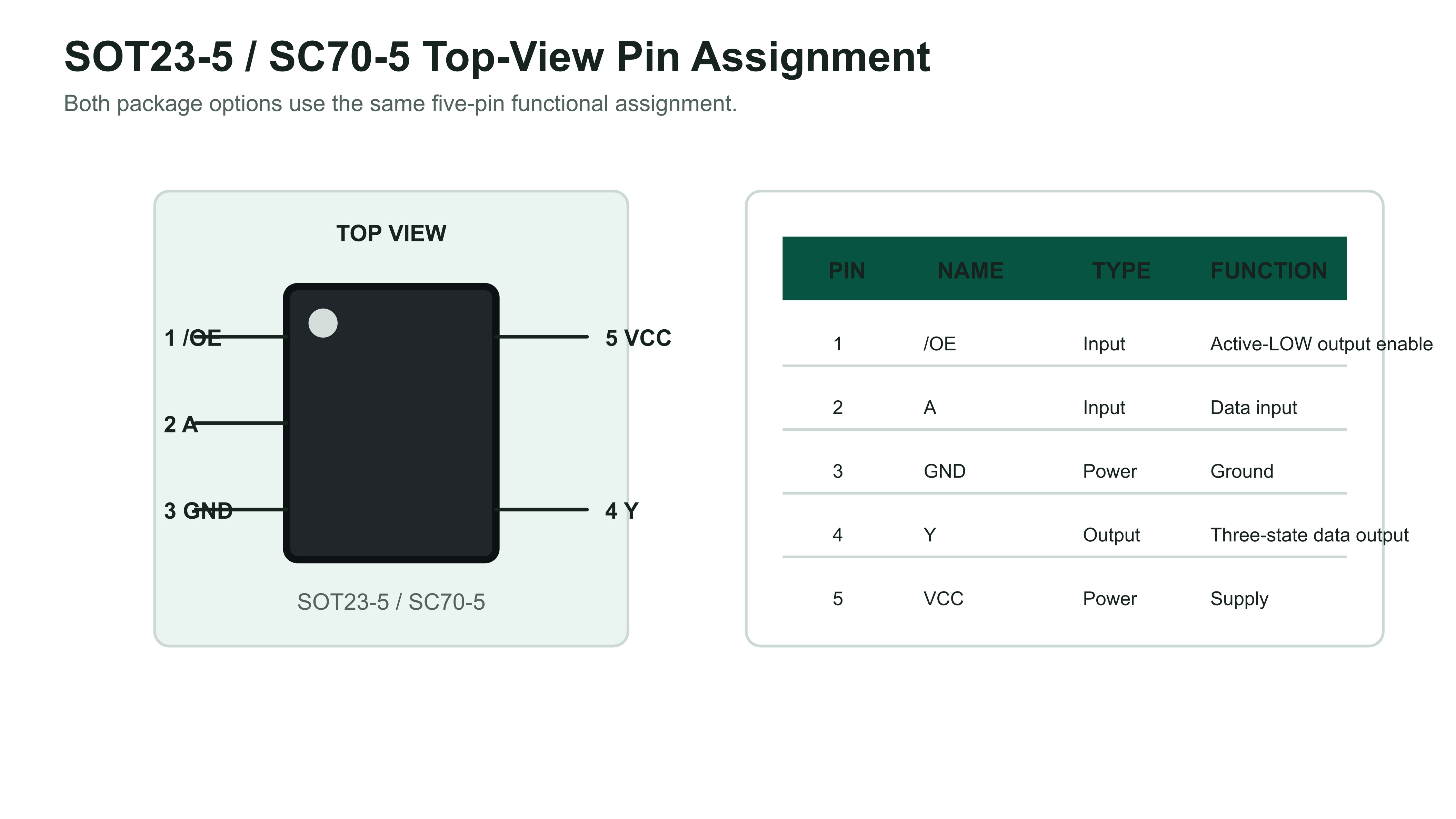
The function table defines three cases. With /OE LOW, Y follows A. With /OE HIGH, A is a don’t-care input and Y is in the high-impedance state.
| Pin | Name | Type | Function | Engineering note |
|---|---|---|---|---|
| 1 | /OE | Input | Active-LOW output enable | Pull HIGH when a defined disabled state is required; size the pull-up for the driver’s sink capability. |
| 2 | A | Input | Noninverting data input | Do not leave floating; observe the applicable VIH/VIL limits. |
| 3 | GND | Power | Ground | Use a short return to the local bypass capacitor. |
| 4 | Y | Output | Three-state push-pull output | Avoid simultaneous drive from another active output. |
| 5 | VCC | Power | Supply | Place local decoupling close to pins 5 and 3. |
Ordering Codes and Package Selection
| Ordering number | Temperature range | Package | Top marking | MSL | Packing |
|---|---|---|---|---|---|
| SN74LVC1G125DCKR | -40 °C to +125 °C | SC70-5 / SOT353 equivalent | CM5 | MSL 3 | Tape and reel, 3,000 units |
| SN74LVC1G125DBVR | -40 °C to +125 °C | SOT23-5 | C255 | MSL 3 | Tape and reel, 3,000 units |
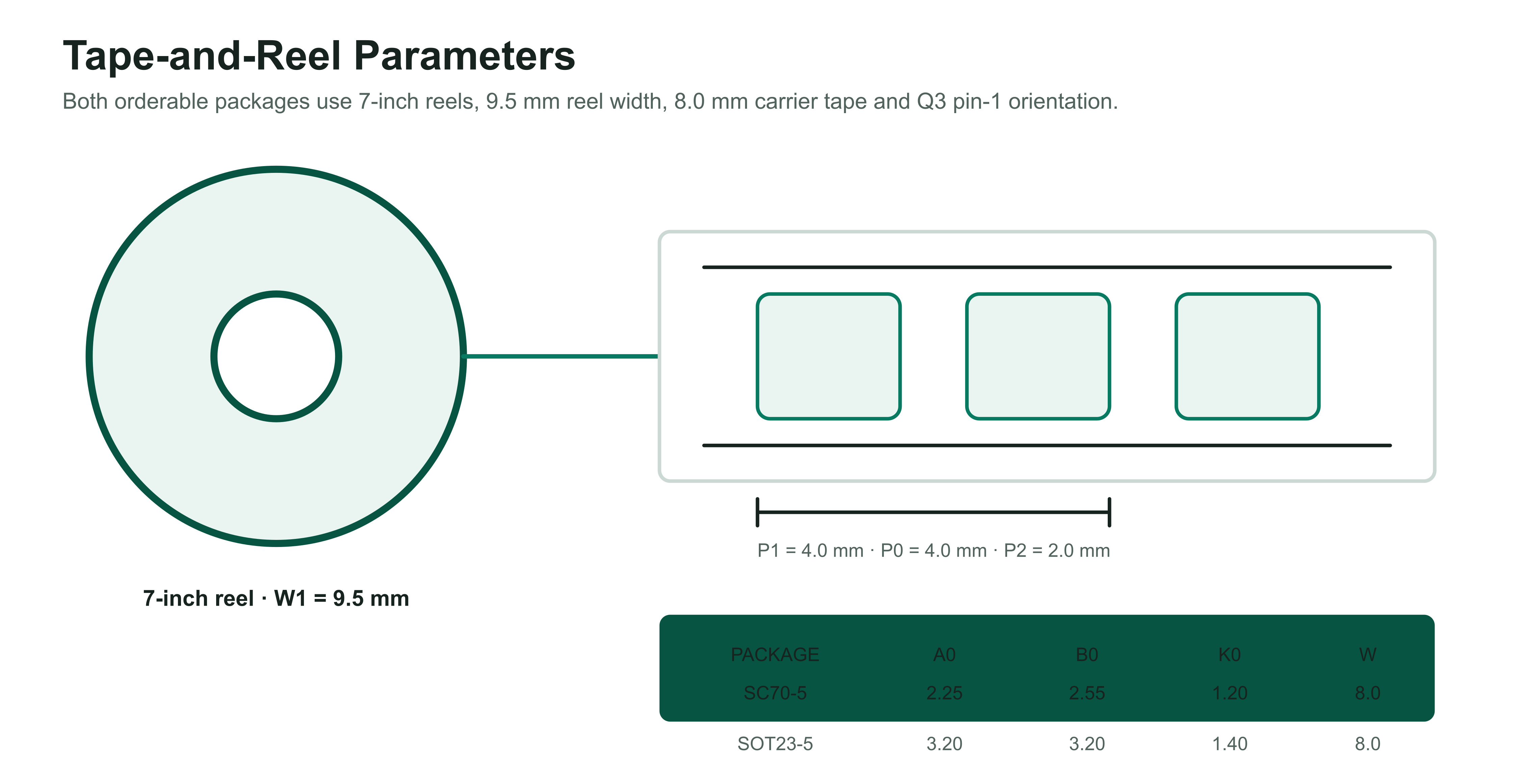
Additional lot, date, vendor, logo or environmental markings may appear. Confirm the full ordering code, five-pin package drawing, top marking and Q3 tape orientation during receiving inspection.
Recommended Operating Conditions and Absolute Limits
Recommended operating conditions define the functional design range. Absolute maximum ratings are stress limits only and do not establish normal operation or long-term reliability.
| Parameter | Condition | Minimum | Maximum | Unit |
|---|---|---|---|---|
| Supply voltage, VCC | Operating | 1.65 | 5.5 | V |
| Supply voltage, VCC | Data retention only | 1.5 | 5.5 | V |
| Input voltage, VI | A or /OE | 0 | 5.5 | V |
| Output voltage, VO | Operating | 0 | VCC | V |
| Input rise/fall, tr or tf | VCC = 1.8 V ±0.15 V or 2.5 V ±0.2 V | - | 20 | ns/V |
| Input rise/fall, tr or tf | VCC = 3.3 V ±0.3 V | - | 10 | ns/V |
| Input rise/fall, tr or tf | VCC = 5 V ±0.5 V | - | 5 | ns/V |
| Ambient temperature, TA | Operating | -40 | 125 | °C |
Absolute maximum and handling limits
| Parameter | Condition | Minimum | Maximum | Unit |
|---|---|---|---|---|
| Supply voltage | VCC | -0.5 | 6.5 | V |
| Input voltage | VI | -0.5 | 6.5 | V |
| Output voltage | High-impedance or power-off state | -0.5 | 6.5 | V |
| Output voltage | HIGH or LOW state | -0.5 | VCC + 0.5 | V |
| Input clamp current | VI < 0 V | -50 | mA | |
| Output clamp current | VO < 0 V | -50 | mA | |
| Continuous output current | IO | ±50 | mA | |
| Continuous VCC or GND current | - | ±100 | mA | |
| Junction temperature | TJ | -65 | 150 | °C |
| Storage temperature | Tstg | -65 | 150 | °C |
DC Characteristics and Logic Levels
Unless otherwise noted, full-range limits apply from -40 °C to +125 °C. Typical values are characterized at +25 °C and are not guaranteed production limits.
| VCC range | VIH minimum | VIL maximum | Engineering interpretation |
|---|---|---|---|
| 1.65 V to 1.95 V | 0.65 × VCC | 0.30 × VCC | Thresholds scale with supply. |
| 2.3 V to 2.7 V | 1.7 V | 0.7 V | Use the fixed guaranteed limits. |
| 3.0 V to 3.6 V | 2.2 V | 0.8 V | Use the fixed guaranteed limits. |
| 4.5 V to 5.5 V | 0.70 × VCC | 0.30 × VCC | Thresholds scale with supply. |
Output levels, leakage and supply current
| Parameter | Test condition | VCC | Temperature | Limit or typical value | Unit |
|---|---|---|---|---|---|
| VOH | IOH = -100 µA | 1.65 V to 5.5 V | Full | Minimum VCC - 0.1 V | V |
| VOH | IOH = -4 / -8 / -16 / -24 / -32 mA | 1.65 / 2.3 / 3.0 / 3.0 / 4.5 V | Full | Minimum 1.2 / 1.9 / 2.4 / 2.3 / 3.8 V | V |
| VOL | IOL = 100 µA | 1.65 V to 5.5 V | Full | Maximum 0.1 V | V |
| VOL | IOL = 4 / 8 / 16 / 24 / 32 mA | 1.65 / 2.3 / 3.0 / 3.0 / 4.5 V | Full | Maximum 0.45 / 0.30 / 0.40 / 0.55 / 0.55 V | V |
| II | A or /OE at 5.5 V or GND | 0 V to 5.5 V | +25 °C / Full | Typical ±0.1 µA / maximum ±5 µA | µA |
| Ioff | VI or VO = 5.5 V | 0 V | +25 °C / Full | Typical ±0.1 µA / maximum ±10 µA | µA |
| IOZ | VO = 0 V to 5.5 V; output disabled | 3.6 V | Full | Maximum 10 µA | µA |
| ICC | VI = 5.5 V or GND, IO = 0 | 1.65 V to 5.5 V | +25 °C / Full | Typical 0.1 µA / maximum 10 µA | µA |
| ΔICC | One input at VCC - 0.6 V; other inputs at VCC or GND | 3 V to 5.5 V | Full | Maximum 500 µA | µA |
AC Switching and Three-State Timing
The Rev A.1 specification lists typical propagation, enable, and disable delays at TA = +25 °C under the stated resistive and capacitive loads. Because the table provides no maximum values, these are characterization data rather than guaranteed worst-case timing limits.
| Parameter | Path | 1.8 V ±0.15 V | 2.5 V ±0.2 V | 3.3 V ±0.3 V | 5.0 V ±0.5 V | Status |
|---|---|---|---|---|---|---|
| tpd | A to Y | 12 ns | 7 ns | 6 ns | 4.3 ns | Typical |
| ten | /OE to Y | 14.9 ns | 7.8 ns | 6.5 ns | 4.8 ns | Typical |
| tdis | /OE to Y | 11.4 ns | 7.4 ns | 5.7 ns | 5.0 ns | Typical |
| Cpd, enabled | f = 10 MHz | 18 pF | 18 pF | 19 pF | 21 pF | Typical |
| Cpd, disabled | f = 10 MHz | 2 pF | 2 pF | 2 pF | 4 pF | Typical |
Specified load: CL = 30 pF and RL = 1 kΩ at 1.8 V; CL = 30 pF and RL = 500 Ω at 2.5 V; CL = 50 pF and RL = 500 Ω at 3.3 V and 5.0 V. CL includes probe and test-fixture capacitance.
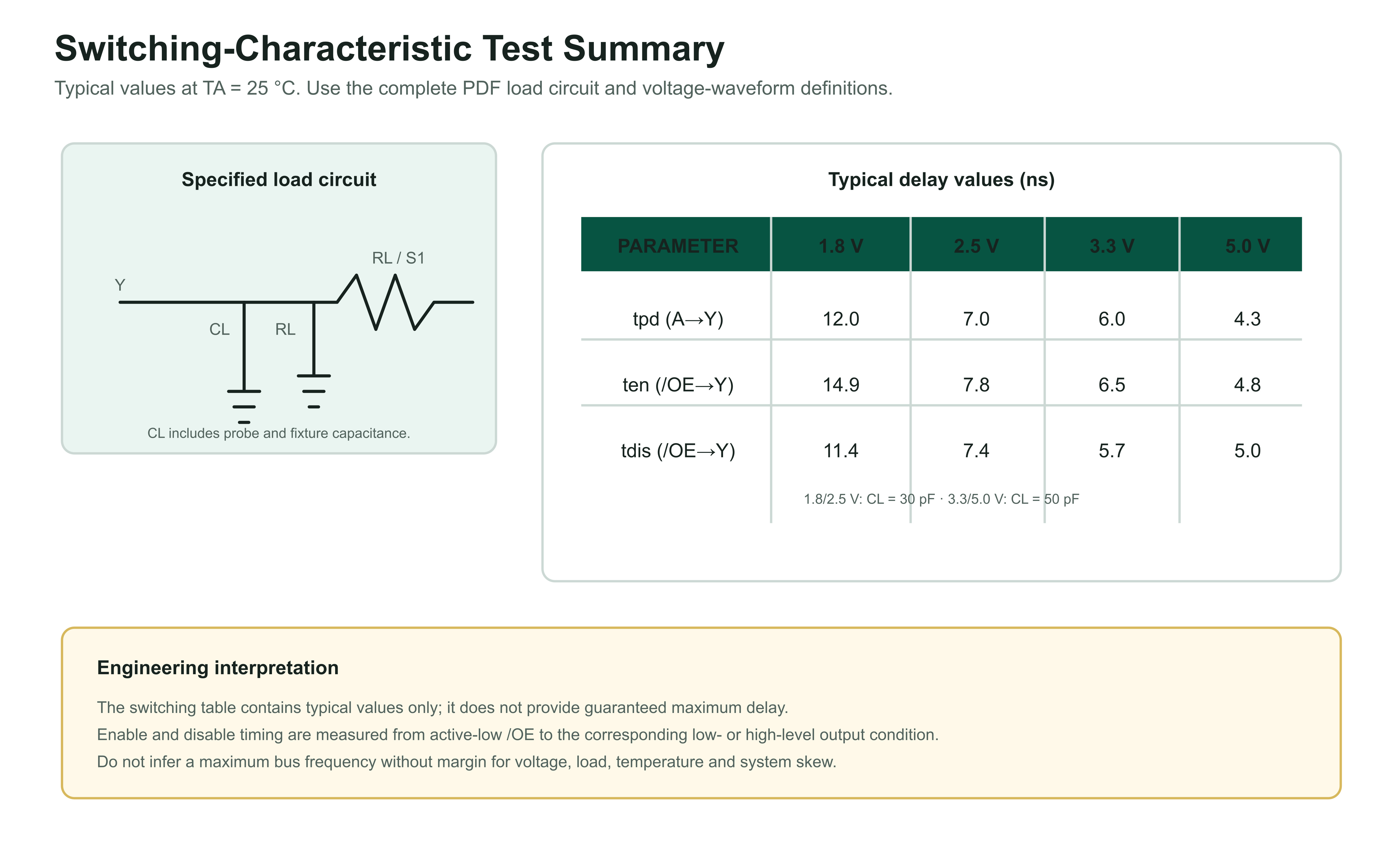
Timing boundary: Account for control-path skew and adequate break-before-make margin when assigning bus ownership. Do not derive a guaranteed maximum bus frequency from typical delay values alone.
Bus Control, Power Sequencing and PCB Layout
The following circuit is application-design guidance rather than a guaranteed reference circuit. Use the electrical and timing tables for component limits, and validate the complete bus and power-distribution network.
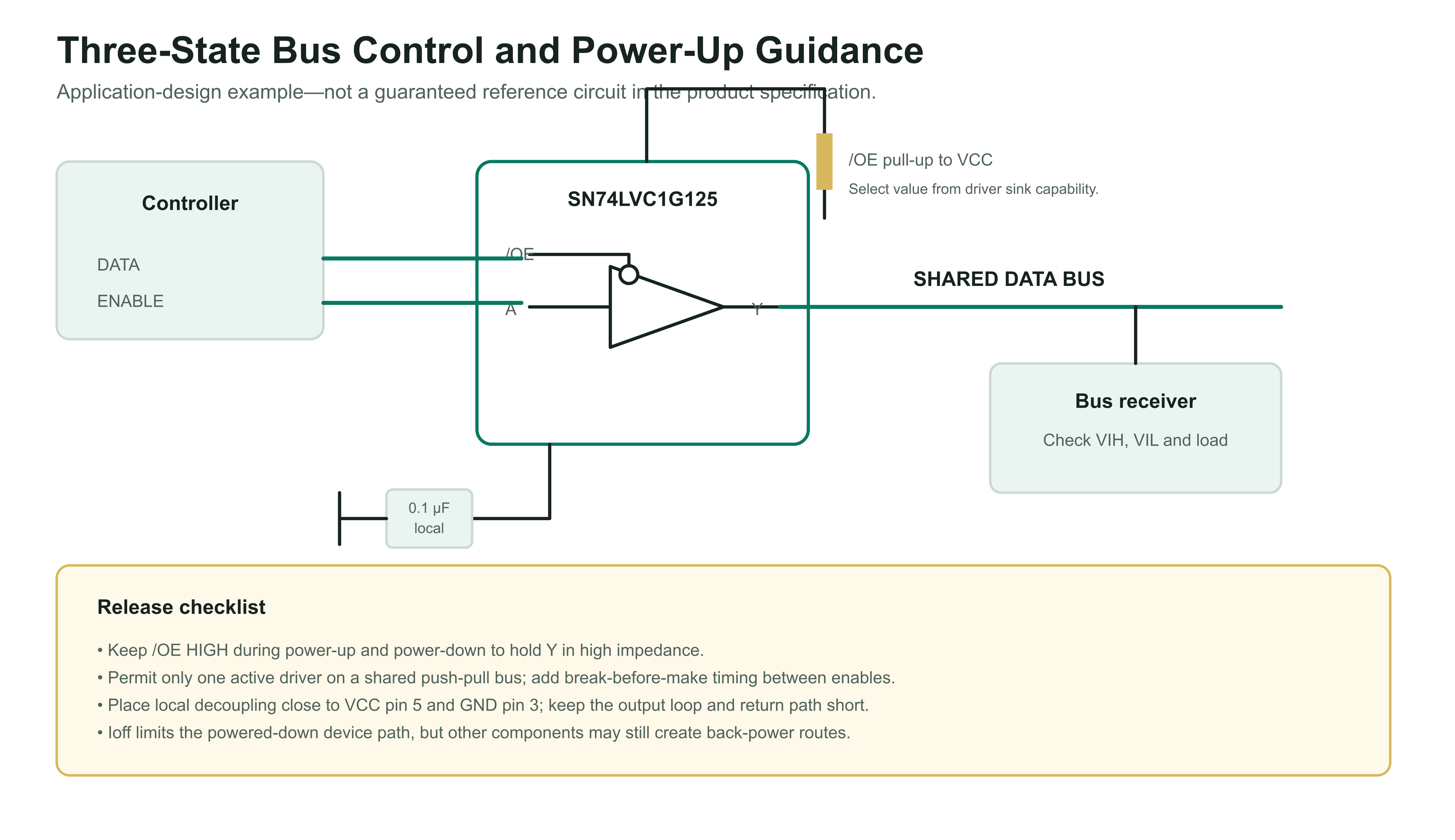
- Default to high impedance: the specification recommends connecting /OE to VCC through a pull-up during power-up and power-down. Determine the minimum resistance from the /OE driver’s current-sinking capability.
- Prevent output contention: use break-before-make sequencing so two push-pull outputs cannot actively drive the shared node at the same time.
- Do not leave A or /OE floating: hold every unused input at VCC or GND.
- Respect edge-rate limits: the maximum tr/tf limit changes from 20 ns/V at the lower supply ranges to 5 ns/V at 5.0 V.
- Budget disabled leakage: include IOZ, receiver leakage, and external bias networks when Y is high impedance.
- Validate partial power-down: Ioff limits current through the device; ESD structures and other board components can still create back-power paths.
SOT23-5 and SC70-5 Packages, Land Patterns and Packing
Both Green 5-pin package options share the same logical pin assignment but have different body dimensions, lead pitches, top markings, and thermal impedances. Do not use one PCB footprint for both packages.
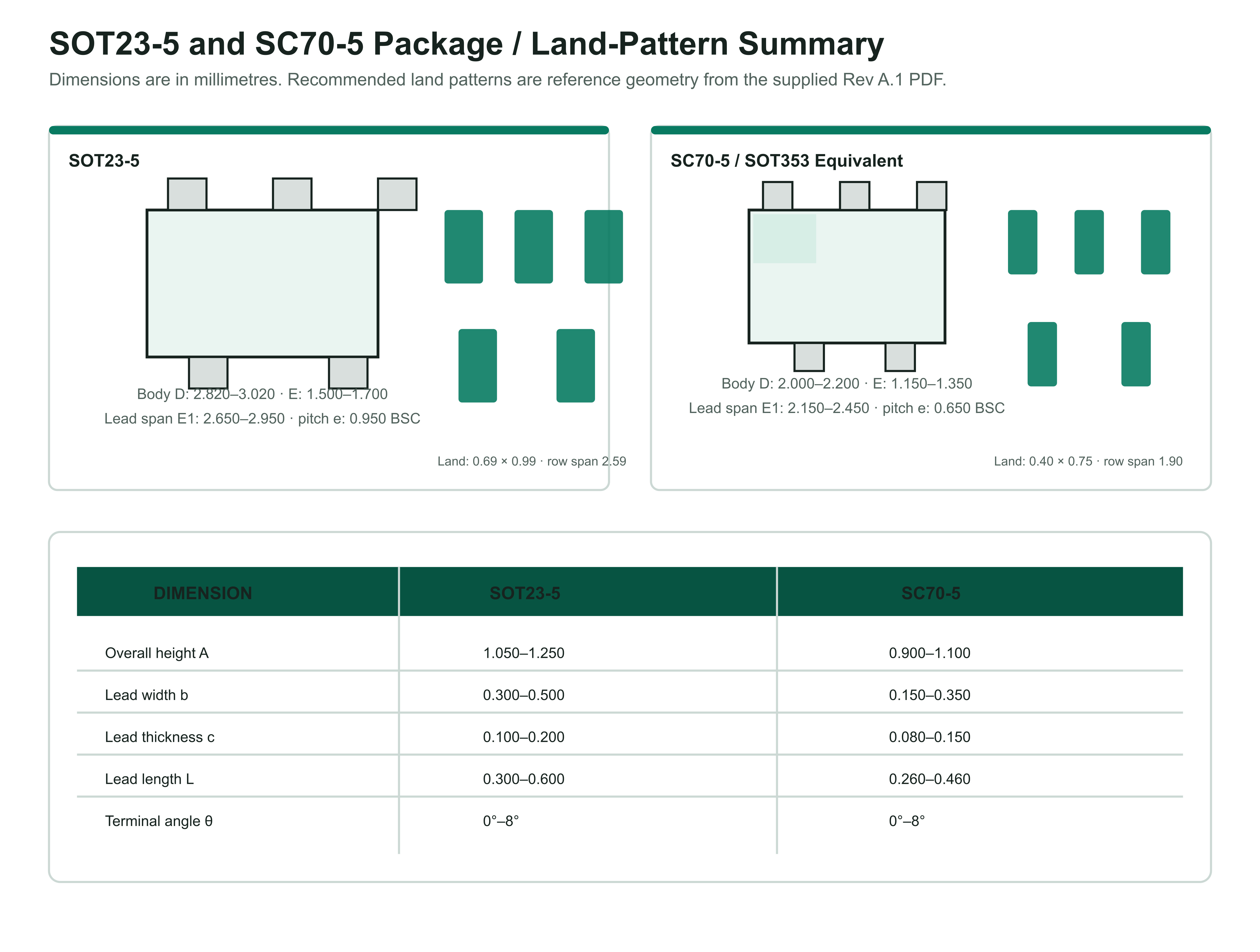
| Dimension | SOT23-5 | SC70-5 | Unit |
|---|---|---|---|
| Overall height A | 1.050 to 1.250 | 0.900 to 1.100 | mm |
| Body length D | 2.820 to 3.020 | 2.000 to 2.200 | mm |
| Body width E | 1.500 to 1.700 | 1.150 to 1.350 | mm |
| Overall lead span E1 | 2.650 to 2.950 | 2.150 to 2.450 | mm |
| Lead pitch e | 0.950 BSC | 0.650 BSC | mm |
| Outer lead pitch e1 | 1.800 to 2.000 | 1.300 BSC | mm |
| Lead width b | 0.300 to 0.500 | 0.150 to 0.350 | mm |
| Lead thickness c | 0.100 to 0.200 | 0.080 to 0.150 | mm |
| Lead length L | 0.300 to 0.600 | 0.260 to 0.460 | mm |
Application Guidance and Design Limitations
The Rev A.1 specification lists AV receivers, cable-modem termination systems, digital picture frames, high-speed data acquisition and generation, high-voltage motor controls, GPS devices, portable media players and video communication systems. These are possible use contexts, not end-product approvals.
 AV ReceiversGate or isolate board-level digital control signals; this device does not process the analog audio path.
 Cable-Modem Termination SystemsProvide controlled digital-path isolation after checking bus ownership, thresholds and load.
 Digital Picture FramesEnable or isolate compact display-control paths while respecting power sequencing.
 Data Acquisition and GenerationControl a unidirectional digital path; validate typical-only timing against system margin.
 High-Voltage Motor ControlsUse only on the low-voltage logic side with required isolation, protection and system qualification.
 GPS Navigation DevicesGate digital control or peripheral-select signals after checking voltage-domain compatibility.
 Portable Media PlayersIsolate a peripheral path to support defined power states and reduce unwanted bus loading.
 Video Communication SystemsControl digital sideband paths; do not treat the device as a high-speed differential video switch.
SN74LVC1G125 Engineering FAQs
What logic function does SN74LVC1G125 implement?
It is a single non-inverting line driver with a 3-state output. When /OE is LOW, Y follows A; when /OE is HIGH, Y is high impedance.
What supply range is recommended?
VCC is specified from 1.65 V to 5.5 V for operation. The separate 1.5 V to 5.5 V entry is data retention only.
Why should /OE be pulled HIGH during power-up and power-down?
A HIGH /OE holds Y in the high-impedance state. The PDF recommends a pull-up to VCC, with the minimum resistor value determined by the current-sinking capability of the /OE driver.
Can the inputs accept 5.5 V when VCC is lower?
The recommended input range is 0 V to 5.5 V. This input tolerance does not by itself make the device a general-purpose level translator; verify output levels and power sequencing.
Is the Y output open-drain or bidirectional?
No. Y is a unidirectional push-pull output when enabled and high impedance when disabled. The device is not an open-drain gate, analog switch or bidirectional bus transceiver.
What typical switching values are listed?
At TA = 25 °C, typical tpd is 12, 7, 6, and 4.3 ns at 1.8, 2.5, 3.3, and 5.0 V. Typical ten is 14.9, 7.8, 6.5, and 4.8 ns; typical tdis is 11.4, 7.4, 5.7, and 5.0 ns.
What do Ioff and IOZ mean?
Ioff limits current through the device when VCC is 0 V. IOZ is the output leakage specification while Y is in its high-impedance state. Neither specification eliminates other board-level back-power paths.
Which packages and ordering codes are listed?
SN74LVC1G125DBVR is SOT23-5 with C255 marking. SN74LVC1G125DCKR is SC70-5, equivalent to SOT353, with CM5 marking. Both are MSL 3 and packed 3,000 units per reel.
Can A or /OE be left floating?
No. Define both logic inputs. The PDF requires all unused inputs to be held at VCC or GND, and /OE should be biased HIGH when a safe disabled state is required.
Do the listed applications establish end-product certification?
No. The application list identifies possible use contexts only. Safety, EMC, reliability, environmental and production qualification remain system responsibilities.
This page is an engineering summary of the SN74LVC1G125 Rev A.1 product specification and does not replace the complete controlled document. Confirm the current revision, ordering code, marking, pin assignment, logic limits, absolute maximum ratings, DC and AC conditions, three-state timing, package tolerances, PCB layout, assembly process and qualification requirements before production release.
