
01 · Device purpose
Product Overview and Selection Scope
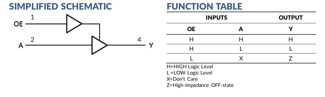
SN74LVC1G126 is a single noninverting bus buffer with a 3-state output. The active-HIGH OE input controls whether Y follows A or disconnects from the bus.
- Wide supply range: 1.65 V to 5.5 V operation.
- 5.5 V input acceptance: A and OE are specified from 0 V to 5.5 V.
- Low static power: 0.1 µA typical ICC at +25 °C under the listed condition.
- Output drive: ±24 mA at VCC = 3.0 V under the stated DC tests.
- Partial power-down: Ioff limits current when VCC is 0 V.
- Compact packaging: SOT23-5 and SC70-5 options.
Selection boundary: This is a digital noninverting buffer, not an analog switch, open-drain driver, Schmitt-trigger input or automatic bidirectional level translator. Verify logic thresholds, output swing, bus ownership and sequencing for the complete system.
02 · Logic and pins
Enable Function, Truth Table and Pin Assignment
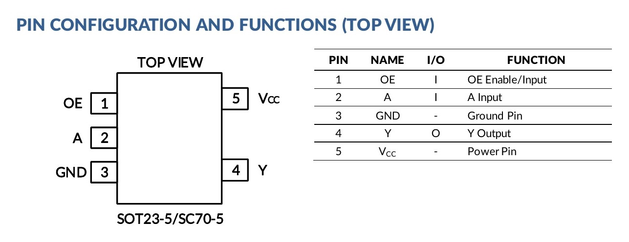
With OE HIGH, the output reproduces input A. Pulling OE LOW places Y in the high-impedance OFF state. For a high-impedance output during power transitions, the source specification recommends tying OE to GND through a pulldown resistor sized for the driving source.
| Pin | Name | Type | Function | Engineering note |
|---|---|---|---|---|
| 1 | OE | Input | Active-HIGH output enable | LOW selects high impedance; define its state during sequencing. |
| 2 | A | Input | Data input | Hold at VCC or GND when unused. |
| 3 | GND | Power | Ground | Use a short local return path. |
| 4 | Y | Output | 3-state noninverting output | Avoid bus contention whenever Y is enabled. |
| 5 | VCC | Power | Supply | Place local bypass capacitance close to pins 5 and 3. |
03 · Orderable options
Ordering Codes and Package Selection
| Ordering number | Temperature range | Package | Top marking | MSL | Packing |
|---|---|---|---|---|---|
| SN74LVC1G126DCKR | -40 °C to +125 °C | SC70-5 / SOT353 equivalent | CNK | MSL 3 | Tape and reel, 3,000 units |
| SN74LVC1G126DBVR | -40 °C to +125 °C | SOT23-5 | C265 | MSL 3 | Tape and reel, 3,000 units |
Additional lot, date, vendor, logo or environmental markings may appear. Confirm the complete ordering code and package drawing during receiving inspection.
04 · Design envelope
Recommended Operating Conditions and Absolute Limits
Recommended conditions define the functional design range. Absolute maximum ratings are stress limits only; operation at those limits is not implied.
| Parameter | Condition | Minimum | Maximum | Unit |
|---|---|---|---|---|
| Supply voltage, VCC | Operating | 1.65 | 5.5 | V |
| Supply voltage, VCC | Data retention only | 1.5 | 5.5 | V |
| Input voltage, VI | Operating | 0 | 5.5 | V |
| Output voltage, VO | Operating | 0 | VCC | V |
| Input transition, tr or tf | VCC = 1.8 V ±0.15 V or 2.5 V ±0.2 V | - | 20 | ns/V |
| Input transition, tr or tf | VCC = 3.3 V ±0.3 V | - | 10 | ns/V |
| Input transition, tr or tf | VCC = 5 V ±0.5 V | - | 5 | ns/V |
| Ambient temperature, TA | Operating | -40 | 125 | °C |
Absolute maximum and handling limits
| Parameter | Condition | Minimum | Maximum | Unit |
|---|---|---|---|---|
| Supply voltage | VCC | -0.5 | 6.5 | V |
| Input voltage | VI | -0.5 | 6.5 | V |
| Output voltage | High impedance or power-off | -0.5 | 6.5 | V |
| Output voltage | HIGH or LOW state | -0.5 | VCC + 0.5 | V |
| Input / output clamp current | VI or VO < 0 V | -50 | mA | |
| Continuous output current | IO | ±50 | mA | |
| Continuous VCC or GND current | - | ±100 | mA | |
| Junction / storage temperature | TJ / Tstg | -65 | 150 | °C |
05 · Static performance
DC Characteristics and Logic Levels
| VCC range | VIH minimum | VIL maximum | Interpretation |
|---|---|---|---|
| 1.65 V to 1.95 V | 0.65 × VCC | 0.30 × VCC | Thresholds scale with supply. |
| 2.3 V to 2.7 V | 1.7 V | 0.7 V | Use the fixed guaranteed limits. |
| 3.0 V to 3.6 V | 2.2 V | 0.8 V | Use the fixed guaranteed limits. |
| 4.5 V to 5.5 V | 0.70 × VCC | 0.30 × VCC | Thresholds scale with supply. |
Output levels, leakage and supply current
| Parameter | Test condition | VCC | Limit or typical value | Unit |
|---|---|---|---|---|
| VOH | IOH = -100 µA | 1.65 V to 5.5 V | Minimum VCC - 0.1 V | V |
| VOH | IOH = -4 / -8 / -16 / -24 / -32 mA | 1.65 / 2.3 / 3.0 / 3.0 / 4.5 V | Minimum 1.2 / 1.9 / 2.4 / 2.3 / 3.8 V | V |
| VOL | IOL = 100 µA | 1.65 V to 5.5 V | Maximum 0.1 V | V |
| VOL | IOL = 4 / 8 / 16 / 24 / 32 mA | 1.65 / 2.3 / 3.0 / 3.0 / 4.5 V | Maximum 0.45 / 0.30 / 0.40 / 0.55 / 0.55 V | V |
| II | A or OE = 5.5 V or GND | 0 V to 5.5 V | ±0.1 µA typical; ±5 µA maximum full range | µA |
| Ioff | VI or VO = 5.5 V | 0 V | ±0.1 µA typical; ±10 µA maximum full range | µA |
| IOZ | VO = 0 V to 5.5 V | 3.6 V | 10 µA maximum full range | µA |
| ICC | VI = 5.5 V or GND, IO = 0 | 1.65 V to 5.5 V | 0.1 µA typical; 10 µA maximum full range | µA |
| ΔICC | One input at VCC - 0.6 V; other inputs at VCC or GND | 3 V to 5.5 V | 500 µA maximum | µA |
06 · Dynamic performance
AC Switching and Test Conditions
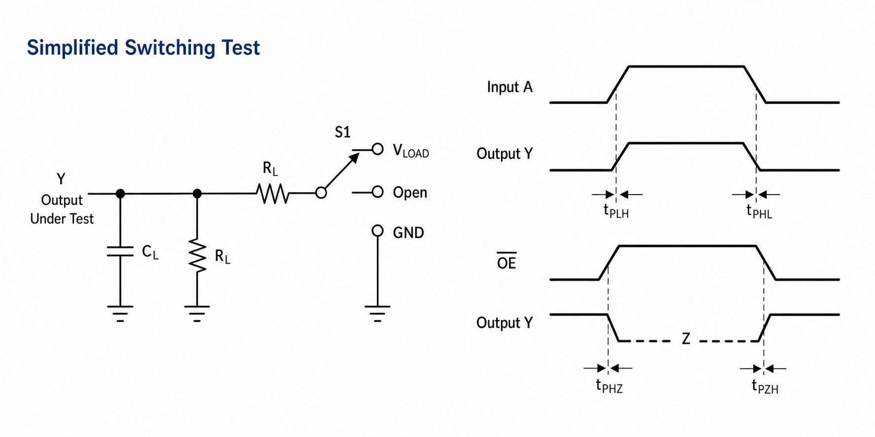
The supplied specification lists typical timing values. No maximum timing values are shown in these tables, so do not treat the numbers as guaranteed worst-case limits.
| Load | Parameter | 1.8 V | 2.5 V | 3.3 V | 5.0 V | Unit |
|---|---|---|---|---|---|---|
| CL = 15 pF | tpd, A to Y | 6.1 | 3.7 | 3.9 | 2.1 | ns typ. |
| CL = 30 pF / 50 pF | tpd, A to Y | 8.6 | 5.3 | 4.0 | 2.9 | ns typ. |
| CL = 30 pF / 50 pF | ten, OE to Y | 9.5 | 5.8 | 5.0 | 3.3 | ns typ. |
| CL = 30 pF / 50 pF | tdis, OE to Y | 7.4 | 4.3 | 4.4 | 3.0 | ns typ. |
| f = 10 MHz | Cpd, output enabled | 18 | 18 | 19 | 21 | pF typ. |
| f = 10 MHz | Cpd, output disabled | 2 | 2 | 2 | 4 | pF typ. |
07 · Implementation
Power Sequencing, OE Control and PCB Guidance
- Define OE during power transitions: use a pulldown to GND when the output must remain high impedance; size it against the driver's current-sourcing capability.
- Do not leave inputs floating: the PDF requires unused inputs to be held at VCC or GND.
- Prevent bus contention: coordinate enable and disable timing so two active outputs do not drive the same node simultaneously.
- Respect edge-rate limits: maximum tr/tf changes from 20 ns/V at low supplies to 5 ns/V at 5 V.
- Validate partial power-down: Ioff limits the IC path, but other components can still back-power the rail.
- Keep the supply loop compact: place local bypass capacitance close to VCC and GND and use short return paths.
System check: Validate enable timing, capacitive load, receiver thresholds, ground bounce, power sequence and bus-fault behavior over production voltage and temperature.
08 · Mechanical
SOT23-5 and SC70-5 Packages, Land Patterns and Packing
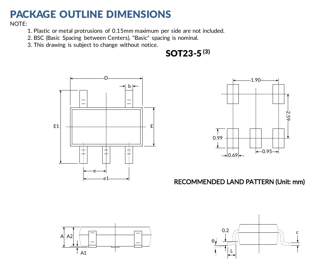
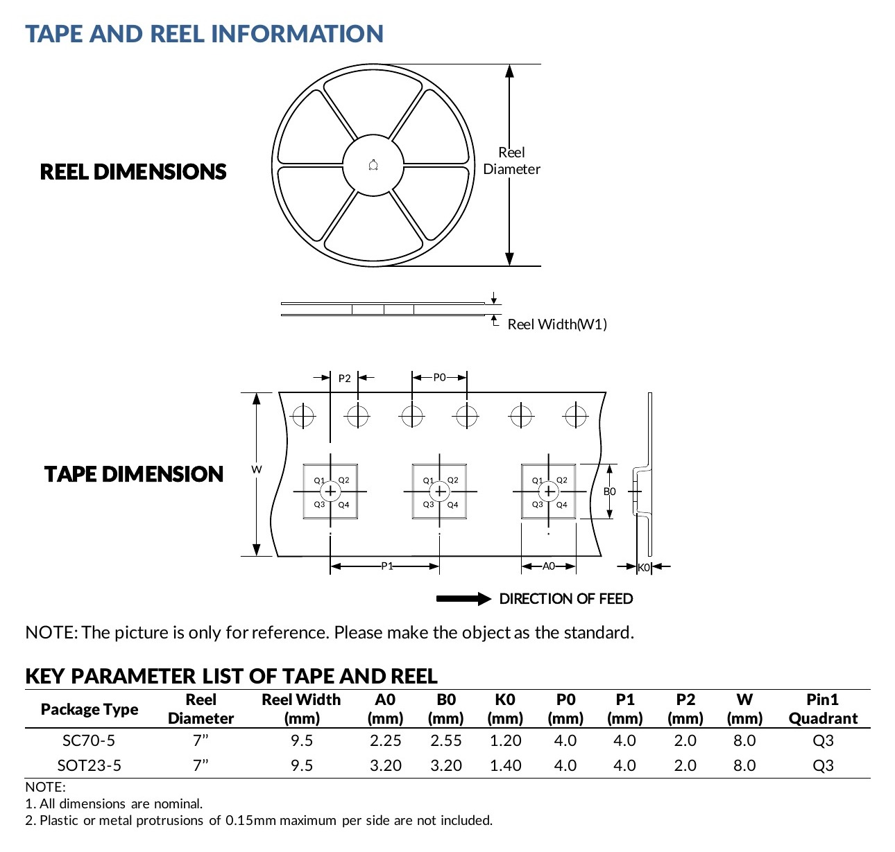
The two packages use the same logical pin assignment but have different body dimensions, lead pitch, top marking and thermal impedance. Do not share one PCB footprint between them.
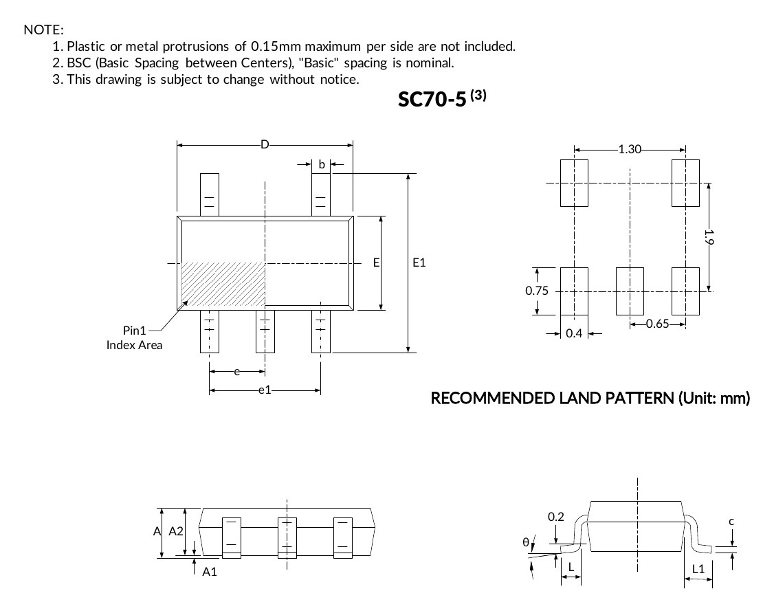
| Dimension | SOT23-5 | SC70-5 | Unit |
|---|---|---|---|
| Overall height A | 1.050 to 1.250 | 0.900 to 1.100 | mm |
| Body length D | 2.820 to 3.020 | 2.000 to 2.200 | mm |
| Body width E | 1.500 to 1.700 | 1.150 to 1.350 | mm |
| Overall lead span E1 | 2.650 to 2.950 | 2.150 to 2.450 | mm |
| Lead pitch e | 0.950 BSC | 0.650 BSC | mm |
| Outer lead pitch e1 | 1.800 to 2.000 | 1.300 BSC | mm |
| Lead width b | 0.300 to 0.500 | 0.150 to 0.350 | mm |
| Lead length L | 0.300 to 0.600 | 0.260 to 0.460 | mm |
09 · Use contexts
Application Guidance and Design Limitations
The supplied specification lists the following application areas. These are use contexts, not end-product approvals or safety certifications.
 AV ReceiversEnable or isolate compact digital control paths.
 Cable Modem Termination SystemsGate shared control or status signals after timing validation.
 Digital Picture FramesProvide compact local buffering and bus isolation.
 Data Acquisition and GenerationBuffer digital controls; validate the listed typical timing against system needs.
 High-Voltage Motor ControlsUse only on appropriately isolated low-voltage logic interfaces.
 Personal Navigation DevicesControl compact low-power digital signal paths.
 Portable Media PlayersEnable or disconnect local board-level logic signals.
 Video Communication SystemsUse for digital control paths, not analog video switching.
10 · Engineering answers
SN74LVC1G126 Engineering FAQs
What function does SN74LVC1G126 implement?
It is one noninverting bus buffer with an active-HIGH OE input and a 3-state Y output.
When is Y high impedance?
Y is high impedance when OE is LOW. When OE is HIGH, Y follows A.
How should OE be handled during power up or power down?
When high impedance is required during transitions, tie OE to GND through a pulldown resistor sized for the current-sourcing capability of the driving source.
What supply range is recommended?
VCC is specified from 1.65 V to 5.5 V for operation. The 1.5 V to 5.5 V entry is data retention only.
Can the inputs accept 5.5 V when VCC is lower?
The recommended input range is 0 V to 5.5 V. Still verify output-level compatibility and every board-level sequencing path.
What are the listed switching values?
At the larger 30 pF or 50 pF loads, typical tpd is 8.6 / 5.3 / 4.0 / 2.9 ns, ten is 9.5 / 5.8 / 5.0 / 3.3 ns and tdis is 7.4 / 4.3 / 4.4 / 3.0 ns at 1.8 / 2.5 / 3.3 / 5.0 V respectively.
What does Ioff provide?
Ioff is specified with VCC = 0 V and VI or VO = 5.5 V, with ±10 µA maximum over the full temperature range.
Which packages are listed?
SN74LVC1G126DBVR is SOT23-5 with C265 marking. SN74LVC1G126DCKR is SC70-5 with CNK marking. Both are MSL 3 and tape-and-reel packed in quantities of 3,000.
Can unused inputs be left open?
No. All unused inputs must be held at VCC or GND.
This page summarizes the supplied SN74LVC1G126 Rev A.1 product specification for component evaluation. Confirm the current controlled specification, ordering code, marking, pin assignment, limits, package tolerances and qualification requirements before production release.