PRACTICAL APPLICATION CASE · ACCESS CONTROL
How to Design a Low-Power Access Control Reader with NF663
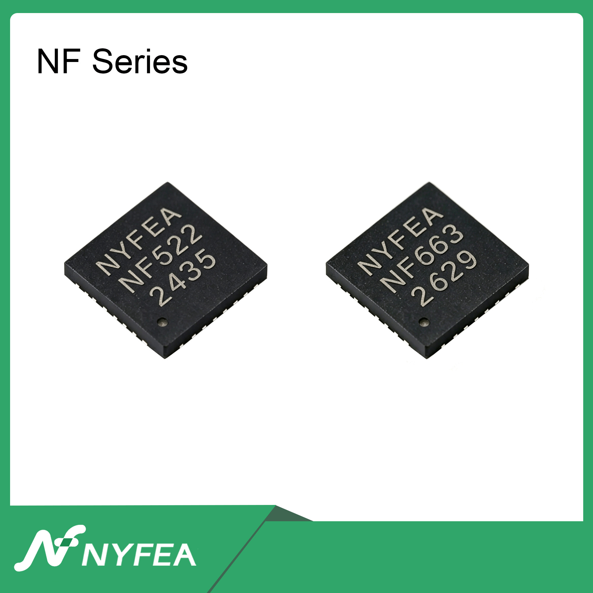
A circuit-level reference case showing how NF663, a host MCU and a 13.56 MHz loop antenna work together from card detection to credential decision.

1. The design objective
The example is a wall-mounted door-access reader. It must detect an ISO/IEC 14443 Type A or Type B credential, exchange the application data with a host MCU, and return to a low-power waiting state after the transaction. The MCU controls the lock decision and the network connection; NF663 is responsible for the 13.56 MHz contactless interface.
| Design item | Reference choice | Reason |
|---|---|---|
| Contactless device | NF663 multi-protocol reader IC | Provides Type A/B reader operation, FIFO, timers, IRQ and low-power card detection |
| Host connection | SPI plus IRQ and PDOWN | Supports deterministic FIFO transfers, event-driven service and controlled sleep/wake |
| Clock | 27.12 MHz crystal at XTAL1/XTAL2 | Provides the clock required by the typical NF663 reader architecture |
| RF interface | Differential TX1/TX2 with an external matching network and loop antenna | Creates the 13.56 MHz magnetic field and couples power/data to the credential |
| Receive path | RXP/RXN pick-off network referenced to VMID | Couples the card load-modulation signal into the NF663 receiver |
| Idle strategy | LPCD-assisted waiting state | Reduces continuous full-field polling in a battery or energy-sensitive terminal |
2. What happens when a card approaches
The application becomes easier to understand when it is followed as one signal and firmware chain rather than as a list of IC features.
- Idle: the MCU places NF663 in the selected low-power waiting strategy. In an LPCD design, the reader periodically evaluates the antenna condition instead of maintaining a continuous full RF field.
- Card detection: a credential entering the antenna region changes the loading seen by the resonant network. The configured detection result causes an NF663 event, and IRQ notifies the MCU.
- Full reader activation: the MCU wakes NF663, loads the required Type A or Type B settings, clears stale FIFO/IRQ state and enables the RF field.
- Poll and anti-collision: NF663 generates the framed polling command. Its differential transmitter drives the antenna through the matching network. If more than one card responds, the host follows the protocol anti-collision and selection sequence.
- Card response: the credential changes the load on the magnetic field. The antenna and receive pick-off network couple this load-modulation signal to RXP/RXN. NF663 demodulates and decodes the response and places the received bytes in its FIFO.
- Host transaction: IRQ signals the MCU, which reads the FIFO over SPI. The MCU then performs the application exchange. If the product uses a secure access module, security-sensitive processing can be assigned to that architecture instead of storing secrets in ordinary application code.
- Door decision: a valid application result causes the MCU to operate a separate lock-driver circuit. The lock, relay or motor driver is outside the NF663 circuit and must include its own power, transient and safety design.
- Recovery: after success, timeout, card removal or protocol error, the MCU switches off the full RF field, clears the transaction state and returns the reader to the defined idle/LPCD state.
Credential ↔ loop antenna (Lant) ↔ matching and receive network ↔ TX1/TX2 and RXP/RXN ↔ NF663 framing/FIFO/IRQ ↔ SPI ↔ MCU ↔ credential decision ↔ external lock driver
3. Complete NF663 smart-lock reference circuit
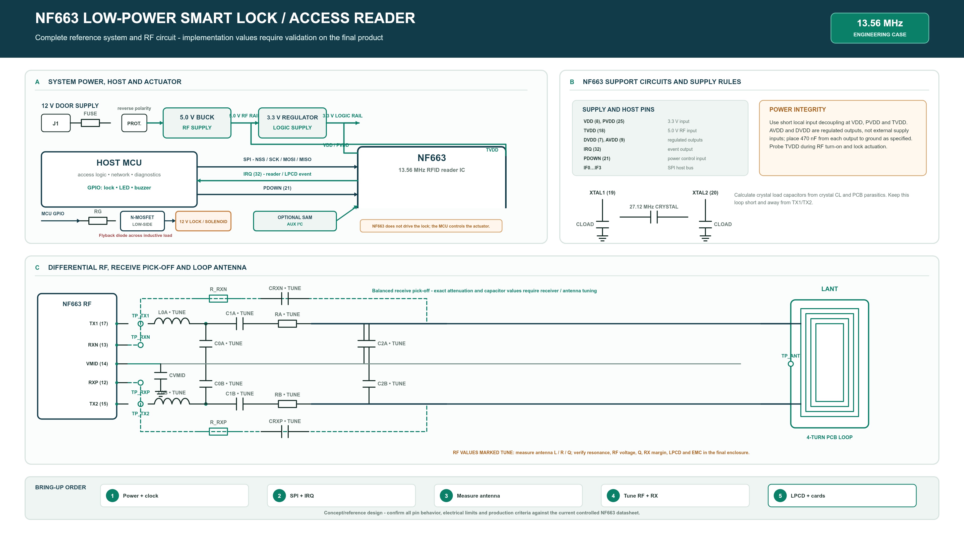
The new diagram below is drawn for this specific case rather than copied from the product specification. It separates the system-level design from the RF network so that power integrity, host control, card detection and lock actuation can be reviewed independently.
Power and lock-actuation domains
The reference system starts from a 12 V door supply. A protected regulator stage creates a 5.0 V RF rail for TVDD and a 3.3 V logic rail for VDD, PVDD and the host MCU. AVDD and DVDD are regulated outputs and require the specified 470 nF local decoupling; they are not external power inputs.
The lock or solenoid is deliberately outside the NF663 boundary. A host GPIO operates a protected low-side MOSFET stage with a flyback path for the inductive load. Probe the NF663 rails during both RF turn-on and lock actuation: a door strike can inject enough supply disturbance to cause intermittent RF range loss or an MCU/reader reset if the power and return paths are not separated correctly.
Host interface, IRQ, PDOWN and the optional secure module
The host-interface pins connect NF663 to the MCU. With SPI selected, the MCU writes commands and configuration and transfers data to and from the 512-byte FIFO. IRQ is the event line: it tells the MCU that a timer expired, data arrived or another enabled reader event occurred. PDOWN gives the host a defined way to enter or leave the power-down state.
The firmware should never treat IRQ as a generic “card detected” line. After every interrupt, read and log the applicable status, error and FIFO information. That distinction is essential when diagnosing a card timeout, CRC error, FIFO condition or low-power wake event.
27.12 MHz crystal: the reader timing reference
XTAL1 and XTAL2 connect to the 27.12 MHz crystal and its load capacitors. Keep the crystal loop short and away from TX1/TX2, the antenna current path and fast MCU clocks. During qualification, confirm oscillator start-up at the intended supply and temperature limits; a reader that starts reliably on one laboratory board may still have inadequate production margin.
TX1/TX2, L0 and C0: differential drive and RF filtering
TX1 and TX2 form the differential transmitter. Each output passes through an L0 element before reaching the first matching node. Together with the C0 shunt capacitors to TVSS, this section contributes to RF filtering and impedance transformation. The symmetrical layout matters: unequal trace length or parasitic capacitance can unbalance the two branches and increase common-mode emissions.
C1, C2, Ra and Lant: resonance, matching and damping
C1 and C2 combine with the antenna inductance Lant and the rest of the network to establish the operating resonance and transform the antenna impedance for the transmitter. Ra provides damping and helps control antenna Q and current. These symbols describe functions, not universal values.
The correct workflow is to measure the fabricated antenna, calculate or simulate starting values, populate the matching network, and then measure the complete board near 13.56 MHz. Final tuning must include card loading, the plastic front cover, metal mounting parts, cables and any display or battery placed near the antenna.
RXP/RXN, CRXP/CRXN and VMID: receive the card response
The receive pick-off samples both antenna branches through a balanced attenuation and AC-coupling network. The exact resistor and CRXP/CRXN values depend on the realized antenna voltage and receiver margin, so they are marked TUNE in the new circuit. VMID provides the receiver bias reference and must be kept quiet with short local routing and filtering.
A strong transmitter field does not prove that reception is robust. During bring-up, record receiver status and error conditions with several credential sizes, orientations and distances. Repeat the test after the reader is mounted on its door, because metalwork, cabling and the front cover can change both antenna tuning and LPCD thresholds.
4. Firmware state machine for the reference reader
| State | NF663/MCU action | Exit condition |
|---|---|---|
| POWER_UP | Verify rails and clock; reset NF663; confirm SPI register access | Reader identity and interface checks pass |
| IDLE_LPCD | RF field off or in the configured low-power detection cycle; MCU sleeps when permitted | LPCD/reader event or scheduled diagnostic |
| RF_START | Wake NF663, load protocol settings, clear FIFO/IRQ, enable transmitter | Field stabilization and configuration complete |
| POLL_SELECT | Send polling command; receive response; perform anti-collision and select one credential | Card selected or timeout/error |
| APPLICATION | Exchange application frames; host or secure architecture evaluates credential | Approved, denied, removed card or protocol error |
| ACTUATE | MCU commands the external lock driver; NF663 is not used to drive the actuator | Door-control timing completed |
| RECOVER | Disable field, clear FIFO/IRQ and errors, record diagnostic result | Return to IDLE_LPCD |
This state-machine approach turns NF663 resources into a diagnosable system. A failed transaction can be traced to power-up, card selection, protocol exchange, security decision or RF recovery instead of being reported only as “card not read.”
5. Bring-up measurements that prove the circuit works
The following sequence is more useful than immediately measuring the farthest card distance:
- Digital bring-up: keep RF off; confirm supply current, PDOWN behavior, 27.12 MHz start-up, SPI read/write, IRQ and timer operation.
- Transmitter check: enable the field; measure TX1/TX2 symmetry, supply droop, antenna waveform and device temperature. Use an appropriate high-impedance or differential probing method.
- Network check: measure resonance and impedance with the intended antenna and PCB. Repeat with the front cover and nearby metal installed.
- Receive check: test several production-representative cards at the intended positions. A high antenna voltage does not prove adequate receive margin.
- Transaction check: run complete credential exchanges, including rapid repeated presentation, edge-of-field operation, two cards, card removal and timeout recovery.
- LPCD check: record no-card and card-present results across enclosure conditions and temperature; then evaluate detection probability, wake time, false wakes and average current.
6. What changes for an industrial ISO/IEC 15693 reader?
The same NF663 host, clock and RF architecture can be the starting point, but the design objective changes. An industrial reader for tools, assets or library tags should be specified by a usable operating area rather than by one best-case distance. The antenna may be larger, the tag population more varied and the installation closer to metal or electrical noise.

Build a position-and-orientation grid, use multiple production tag designs, run nearby motors and DC/DC converters, and test any required multi-tag sequence. Retune the network for that antenna and application. The access-control values from the reference circuit are not automatically the correct industrial values.
7. Why this is relevant to engineers searching for a CLRC663 alternative
CLRC663 is a familiar reference for multi-protocol 13.56 MHz frontend designs. Engineers searching for a CLRC663 alternative are usually trying to solve an application problem: protocol coverage, host integration, low-power operation, antenna design or supply strategy.
NF663 belongs in that evaluation because it targets this same type of reader architecture. The useful comparison is the circuit and system workflow described above—not a copied parameter table. For an existing PCB, confirm pin functions, supply domains, interface selection, initialization and RF values on the target hardware before release.
Engineering FAQs
What does NF663 do in this access-control example?
NF663 creates the 13.56 MHz reader field, frames and decodes the supported contactless protocol, transfers data through its FIFO and reports events to the host MCU. The MCU makes the application decision and controls the separate lock driver.
Why is a 27.12 MHz crystal used for a 13.56 MHz reader?
The typical NF663 architecture uses a 27.12 MHz clock reference from which the reader timing and 13.56 MHz carrier operation are derived. The crystal network must meet the NF663 specification and start reliably in the final product.
Can the capacitor and inductor values in this circuit be copied to any antenna?
No. L0, C0, C1, C2, Ra and the receive-network values interact with the actual antenna inductance, PCB parasitics, enclosure and target compliance requirements. Use the diagram as a topology and determine final values by calculation and measurement.
How does LPCD reduce power?
LPCD allows the reader to look for a change in antenna loading without maintaining continuous full-power polling. The thresholds and timing must be calibrated on the final reader assembly to balance detection and false wakes.
Can NF663 be considered when evaluating CLRC663-class readers?
Yes. NF663 is relevant to multi-protocol 13.56 MHz reader designs with similar application requirements. Compare the required protocols, power domains, host interface and RF implementation, and qualify the target board.
Evaluate NF663 with the real antenna and credential set
For a useful review, provide the antenna dimensions, PCB stack-up, enclosure, supply architecture, host interface and target cards or tags. These inputs allow the reference circuit to become an application-specific design.