Hardware design + public project analysis · 13.56 MHz NFC
CLRC66303HNY Hardware Design: From SPI Bring-Up to NFC Command Writes
CLRC66303HNY board not responding, producing no RF field, or writing a command that never executes? Start with the symptom below. Each path identifies what to measure, how to interpret the result and what to retest after a correction.
For a new board, begin with one stable version-register read. Use the hardware references when a measurement points to the supply, clock or RF network.
Full guide: troubleshooting, hardware references and NF663 evaluation
Start here: get a stable CLRC66303HNY register response
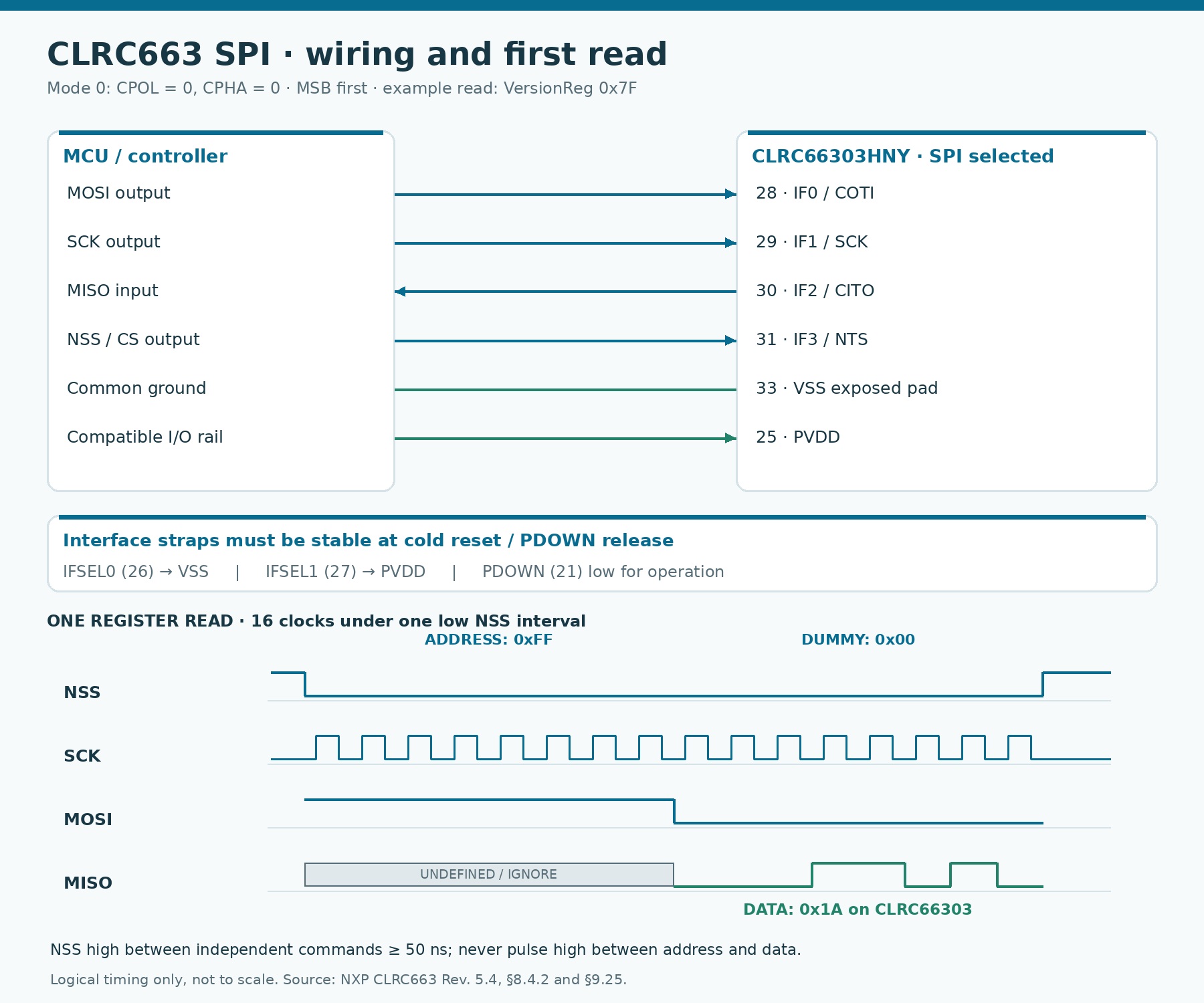
SPI selection occurs after cold reset, power-up or hard-power-down exit. Strap IFSEL0 to VSS and IFSEL1 to PVDD, keeping both stable through interface detection.
NXP’s COTI, CITO and NTS correspond to MOSI, MISO and active-low NSS/CS in this guide.
| MCU / board connection | CLRC66303HNY terminal | Check before the first read |
|---|---|---|
| MOSI | IF0 / COTI, pin 28 | MCU output to reader input. |
| SCK | IF1 / SCK, pin 29 | Idle low; verify at the reader pin. |
| MISO | IF2 / CITO, pin 30 | Reader output to MCU input; avoid bus contention. |
| NSS / CS | IF3 / NTS, pin 31 | Active low; idle high; one continuous frame per command. |
| Mode straps | IFSEL0 pin 26 → VSS; IFSEL1 pin 27 → PVDD | Confirm levels during power-up or PDOWN release. |
| Control / reference | IRQ pin 32; PDOWN pin 21; PVDD pin 25; VSS pad 33 | Common ground and compatible logic levels; PDOWN low for operation. |
 Open full-size JPG ↗
Use SPI Mode 0, MSB first
Set CPOL = 0 and CPHA = 0: SCK idles low; data is sampled on rising edges. Begin around 100 kHz. The datasheet maximum is 10 Mbit/s, subject to board timing and signal integrity.
Set the interface straps before power-up. Apply the rails, keep NSS high and sequence PDOWN as specified. Confirm power and clock startup before reading a register; use documented timing and a finite host timeout.
Read VersionReg before attempting card detection
Read VersionReg at 0x7F using (address << 1) | 1 plus a dummy byte. Transmit 0xFF, 0x00; discard the first MISO byte and read the value from the second.
CLRC66303 returns 0x1A; CLRC66301/02 use 0x18. This checks register communication and revision, not RF performance or authenticity. For unexpected values, follow the SPI fault checks.
Keep NSS low across both bytes and high for at least 50 ns between commands. Disable MCU NSS pulses that would split the transaction.
SPI returns 0x00 / 0xFF: follow the captured signal
Capture NSS, SCK, MOSI and MISO at the reader pins during one version read. Choose the first failed check below; a constant byte alone does not identify a damaged IC.
- No SCK at the reader? Check that the MCU transfer starts, the pin multiplexer selects SPI and the SCK connection reaches pin 29. Retest until the requested frame appears at the IC.
- NSS rises between bytes, or MOSI is not FF 00? Correct the mode, bit order and address framing; use continuous software-controlled NSS across the transfer. Compare the next capture with the timing figure.
- The frame is correct, but MISO stays fixed? Check power at the IC, PDOWN and IFSEL levels at startup, then MISO continuity and competing drivers. Repeat the same read after each correction.
- The trace contains 1A, but firmware reports another value? Inspect the second receive byte and buffer handling. If failures appear only with RF active, capture the supply disturbance before changing SPI settings.
Ready to continue: repeated reads return 0x1A across fresh power-ups. Save the trace and observed byte; then proceed to RF diagnosis.
Source: NXP CLRC663 Rev. 5.4, §8.4.2, Tables 16 and 20, and §9.25 Version register.
Core C code for CLRC663 SPI register access
Use the supplied C99 driver for single-register reads and writes. After adapting the board_hal_* functions and completing startup, call the version check:
uint8_t observed = 0;
int status = clrc66303_check_version(&observed);
/* status ==  0: observed is 0x1A (CLRC66303)
 * status == -1: SPI transfer failed
 * status == -2: read succeeded; inspect the other version byte
 */
Show the complete register driver and MCU adaptation points
/* CLRC66303 SPI register access example, C99.
 * Adapt every board_hal_* function to the target MCU.
 * Configure SPI mode 0, MSB first, initially 100 kHz (bring-up choice).
 * This is a transport example, not a complete NFC protocol driver.
 */
#include <stdbool.h>
#include <stddef.h>
#include <stdint.h>

/* Blocking transfer; return only after the last SCK edge.
 * Return false on timeout/error. Do not toggle NSS inside this function.
 */
extern bool board_hal_spi_transfer(const uint8_t *tx, uint8_t *rx,
                                   size_t length);
extern void board_hal_nss(bool high);
/* Meet the datasheet NSS-high interval: at least 50 ns.
 * Account for GPIO, timer and compiler behavior on the actual MCU.
 */
extern void board_hal_nss_high_gap(void);

#define CLRC663_VERSION_REG       UINT8_C(0x7F)
#define CLRC66303_EXPECTED_VERSION UINT8_C(0x1A)

/* Serialize access to this SPI bus for the whole transaction. */
static bool clrc663_frame(const uint8_t tx[2], uint8_t rx[2])
{
    board_hal_nss(false);
    const bool ok = board_hal_spi_transfer(tx, rx, 2u);
    board_hal_nss(true);       /* Release NSS even after a bus error. */
    board_hal_nss_high_gap();
    return ok;
}

bool clrc663_read_reg(uint8_t reg, uint8_t *value)
{
    if (reg > UINT8_C(0x7F) || value == NULL) {
        return false;
    }
    const uint8_t tx[2] = {
        (uint8_t)((reg << 1u) | 1u),  /* LSB = 1: read. */
        UINT8_C(0x00)                /* Dummy byte generates clocks. */
    };
    uint8_t rx[2] = {0u, 0u};
    if (!clrc663_frame(tx, rx)) {
        return false;
    }
    *value = rx[1];             /* Address-phase MISO is not the value. */
    return true;
}

bool clrc663_write_reg(uint8_t reg, uint8_t value)
{
    if (reg > UINT8_C(0x7F)) {
        return false;
    }
    const uint8_t tx[2] = {
        (uint8_t)(reg << 1u),   /* LSB = 0: write. */
        value
    };
    uint8_t rx[2] = {0u, 0u};
    return clrc663_frame(tx, rx);
}

/* Call after valid rails, settled IFSEL straps and PDOWN release.
 *  0 = expected CLRC66303 version; -1 = bus error; -2 = other version.
 * Log the observed byte; VersionReg is not an authenticity test.
 */
int clrc66303_check_version(uint8_t *observed)
{
    uint8_t version = 0u;
    if (!clrc663_read_reg(CLRC663_VERSION_REG, &version)) {
        return -1;
    }
    if (observed != NULL) {
        *observed = version;
    }
    return version == CLRC66303_EXPECTED_VERSION ? 0 : -2;
}
Download the core C source (TXT) · The package also includes a host-side framing test.
Adapt the blocking HAL functions, preserve the full NSS frame and serialize shared-bus access. Use the signal checks above to separate a framing error from a board fault. This driver does not implement card polling, FIFO/IRQ handling or anticollision.
Reference: NXP AN12657, operation without a library. The example passed host-side syntax/framing checks; hardware validation remains required.
Registers respond, but there is no RF field: isolate the failing stage
Log the board revision, firmware, supply, antenna and card. Change one variable at a time and resolve the first failing stage in the sequence below.
Download the bring-up record to log expected results, observations and next actions.
Prerequisites: valid rails, defined reset/interface selection, a running clock and stable register reads. Keep the board, firmware, card and antenna configuration fixed while comparing measurements.
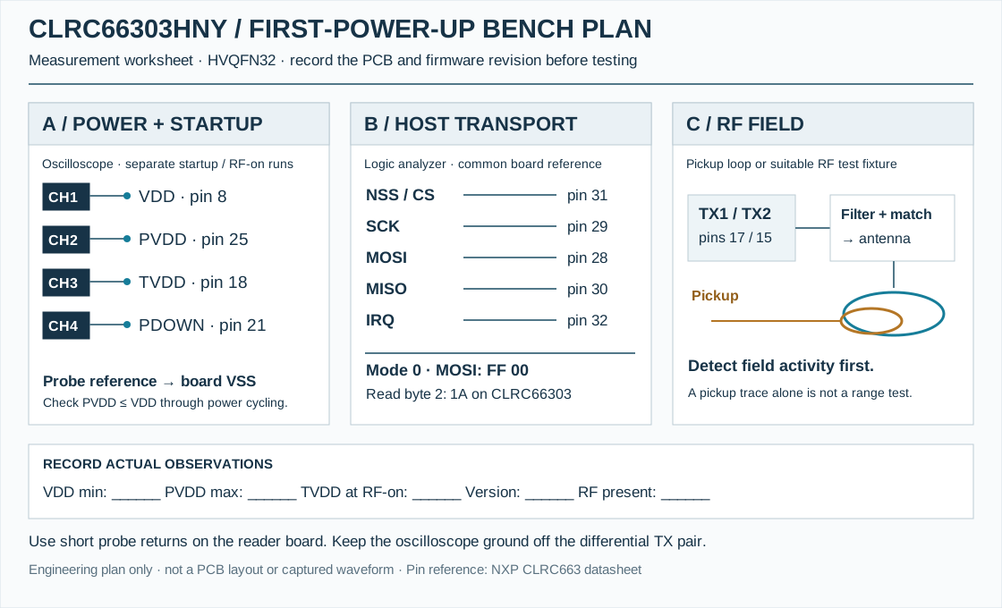 Open the engineering measurement plan ↗
Find where the RF path stops
Request field activation with the intended protocol configuration. Capture TVDD during the attempt and check RF activity using an appropriate differential or near-field fixture. Never connect a grounded probe across TX1/TX2.
- TVDD falls or register communication becomes unstable: resolve supply capacity, local decoupling and ground-return issues first. Repeat field activation and confirm the rail stays within its operating limits.
- TVDD is stable, but no TX activity is observed: inspect oscillator operation, transmitter-enable configuration and command/error status. Confirm host writes reached the intended registers before editing the antenna network.
- TX activity exists, but the antenna has little field: follow the filter-to-antenna path. Check population, solder joints and coil continuity with power off; assess matching under controlled conditions. Compare signals before and after the affected stage.
- The antenna has a field, but the card stays silent: move to protocol and receiver checks below. Field presence alone does not verify modulation, receive sensitivity or a valid polling sequence.
Retest: field activation is repeatable without supply collapse; a known supported card completes the intended exchange at a fixed position. Record attempts, successful exchanges and errors before testing range.
Field present? Use the next symptom
| Observed symptom | Measure first | Next action / pass criterion |
|---|---|---|
| Field present; no card response | Known supported card, polling frame, IRQ/errors and FIFO data. | Select the card's protocol. If the frame is correct, inspect RXP/RXN and VMID. Retest a complete exchange at the same position. |
| ATQA received; no UID | First failed anticollision/select exchange, receive length and timeout. | Use the STM32 UID troubleshooting guide to check cascade handling, CRC and parity. |
| Works bare; fails in enclosure | Same card position, supply and firmware before/after assembly. | Add the housing, metal plate and cable separately. Check supply changes and remeasure antenna impedance when performance shifts; retest the required operating region. |
References: NXP AN12657 for command-level operation; AN11019 for the RF network. Related: CLRC663 register and LPCD troubleshooting.
What is CLRC66303HNY, and what does HNY mean?
CLRC66303HNY is an ordering variant of NXP’s CLRC66303 NFC frontend. It handles RF and reader functions for ISO/IEC 14443 A/B, ISO/IEC 15693 and other documented modes; the host runs protocol and application software.
| Identifier | Meaning in this design |
|---|---|
| CLRC66303 | The CLRC663 plus device version. Do not assume CLRC66301 or CLRC66302 has identical analog limits or startup behavior. |
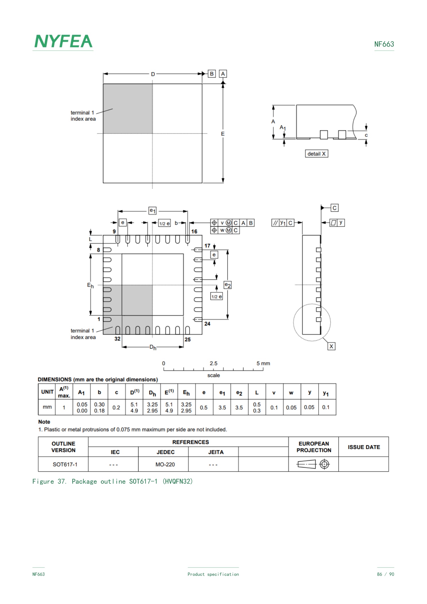
| HN package | HVQFN32, NXP package outline SOT617-1, nominal body 5 × 5 × 0.85 mm, with wettable flanks. |
| HNY ordering variant | The HN device supplied on a 6,000-piece reel in the current ordering table. HNE and HNK are tray-based delivery variants. |
| Top-side marking | The device-identification line is 66303; other lines encode manufacturing traceability. The complete ordering string need not be printed on the chip. |
Keep the complete ordering code on the BOM. Check package, packing label and lot traceability at incoming inspection; a similar top mark cannot identify the reel variant.
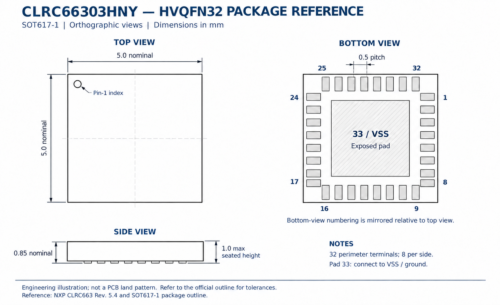 Open full-size PNG ↗
Sources: NXP CLRC663 plus product overview; CLRC663 Rev. 5.4, ordering information and §15 package marking.
CLRC66303HNY pinout: HVQFN32 pin groups and pad 33
The package has 32 perimeter terminals and exposed center pad 33. Connect pad 33 to VSS. Include it in both the schematic symbol and PCB footprint.
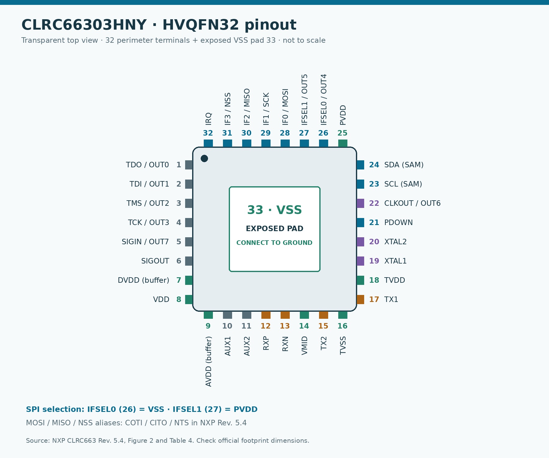 Open full-size JPG ↗
Host and control
IF0–IF3: 28–31 · IFSEL0/1: 26/27IRQ: 32 · PDOWN: 21
Interface signals are multiplexed. Their function depends on the selected host mode. Route IRQ and PDOWN deliberately rather than treating them as spare GPIOs.
Clock
XTAL1: 19 · XTAL2: 20 · CLKOUT: 22Use the clock checks when startup or command timing is intermittent.
Power and ground
VDD: 8 · PVDD: 25 · TVDD: 18AVDD: 9 · DVDD: 7 · TVSS: 16 · VSS: 33
Use the power-domain map to distinguish external rails from regulator buffer nodes.
Transmit and receive
TX1: 17 · TX2: 15RXP: 12 · RXN: 13 · VMID: 14
The differential transmit network and biased receive path form an RF system. RXP/RXN must not be treated as ordinary digital inputs.
SCL/SDA pins 23/24 belong to the separate SAM interface. Auxiliary/test functions use pins 1–6, 10 and 11; consult the pin map and NXP’s unused-pin guidance before assigning pull resistors.
Source: NXP CLRC663 Rev. 5.4, §7 and Table 4. The HVQFN32 mapping must not be applied to the VFBGA36 variant.
How to connect VDD, PVDD, TVDD, AVDD and DVDD
VDD, PVDD and TVDD are external inputs that may share a suitable source. AVDD and DVDD are internal regulator buffer nodes requiring the capacitors shown below.
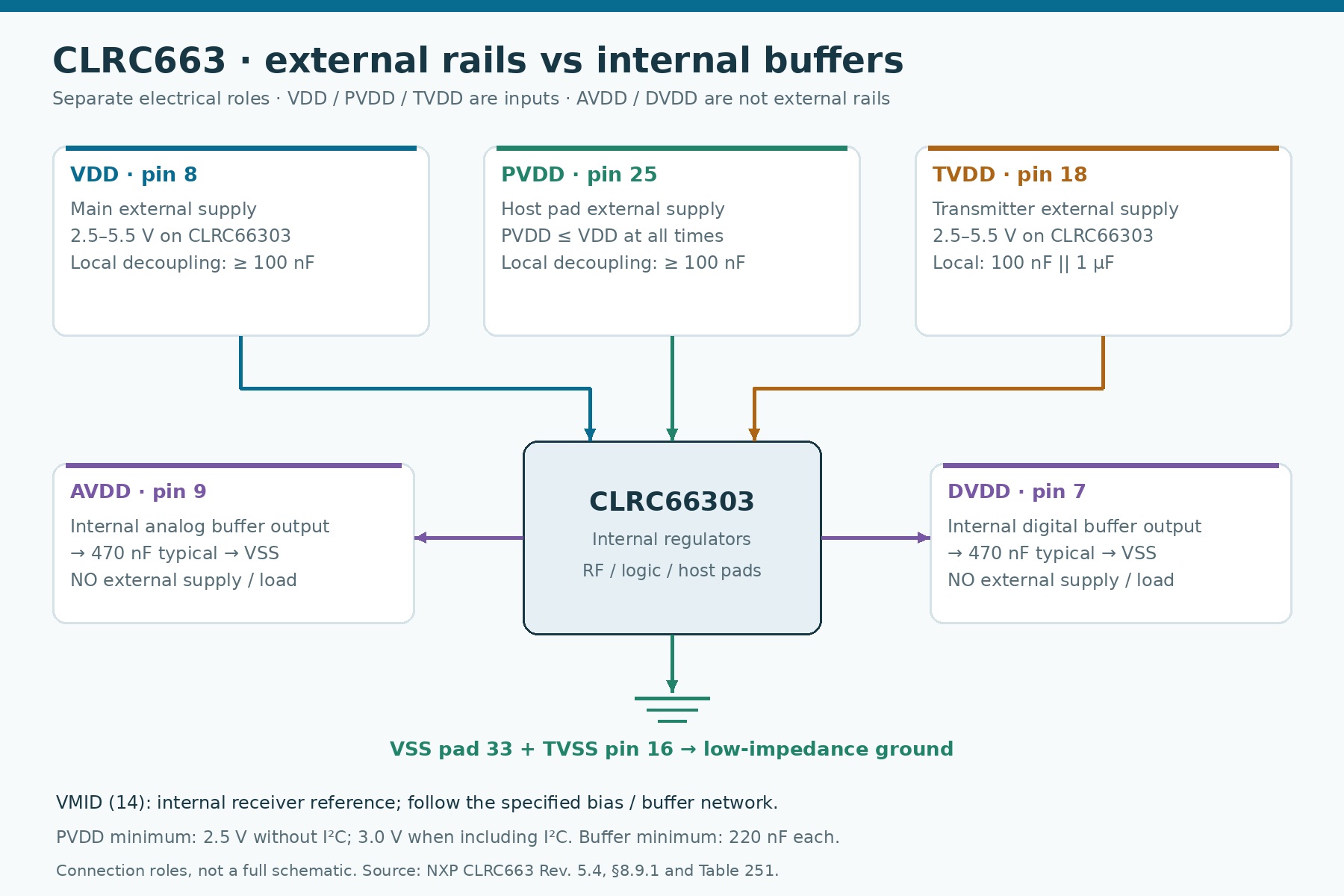 Open full-size JPG ↗
VDD · pin 8
Provide at least 100 nF local decoupling according to the supply-concept guidance. Check this rail at the IC pin, not only at the regulator output.
PVDD · pin 25
PVDD supplies the host pads. Keep PVDD ≤ VDD during operation, startup and shutdown. A 3.3 V MCU can use VDD = PVDD = 3.3 V. Add at least 100 nF local decoupling.
TVDD · pin 18
NXP shows 100 nF in parallel with 1 µF locally. Add board-level storage as needed and check TVDD for voltage drop when the field starts.
AVDD / DVDD · pins 9 / 7
Do not connect these nodes to an external supply or use them to power other circuitry. NXP's supply concept uses 470 nF on each node; the electrical table specifies a 220 nF minimum buffer capacitance.
VMID · pin 14
VMID is not another external supply input. Follow the receiver circuit and keep its return quiet; transmitter-current voltage drop should not contaminate the receive reference.
TVSS / VSS · pins 16 / 33
Connect the center pad with a low-impedance ground structure and appropriate thermal vias. Avoid a long common neck shared by RF return current and sensitive clock or receive components.
CLRC66303 VDD and TVDD support 2.5–5.5 V. PVDD supports 2.5–5.5 V outside I²C operation; its minimum including I²C is 3.0 V. Apply the full operating and sequencing limits.
Measure VDD and PVDD together during startup. At field activation, capture TVDD minimum voltage, ripple and current step at pin 18 with a short probe return.
The HVQFN32 ambient range is −40 to +105 °C under specified PCB and exposed-pad conditions. Check junction temperature, transmitter dissipation and the assembled thermal path.
Source: NXP CLRC663 Rev. 5.4, §8.9.1, Table 251 and the regulator characteristics. Measurement sequence is engineering guidance, not a reported board test.
27.12 MHz crystal selection, layout and safe probing
Connect the 27.12 MHz crystal to XTAL1/XTAL2, pins 19/20. The RF carrier is 13.56 MHz; a crystal at that lower frequency is unsuitable.
NXP specifies 10 pF typical crystal load, 100 Ω maximum ESR and 100 µW maximum drive. Also check frequency tolerance and oscillator operating conditions.
Estimate CL ≈ (C1 × C2) / (C1 + C2) + Cstray, including pad, trace and IC capacitance. Select components for the actual crystal and verify startup margin on the assembled board.
Place the clock loop first
Put the crystal and load components close to pins 19/20. Keep connections short and symmetric where practical. Do not route SCK, TX1/TX2 or switching-regulator nodes through the crystal area.
Check the clock without disturbing it
Probe capacitance can reduce oscillation amplitude or stop startup. Use a suitable low-capacitance probe, or check a correctly configured CLKOUT signal. Record whether connecting the probe changes the symptom.
PDOWN high stops the oscillator. Check that it is low and startup timing has elapsed. For intermittent oscillation, inspect supply ramp, loading, contamination and crystal placement.
Sources: NXP CLRC663 Rev. 5.4, Table 44 and power-down behavior; NXP AN14518, Crystal Oscillator Design Guide. Layout and probing recommendations require verification on the target board.
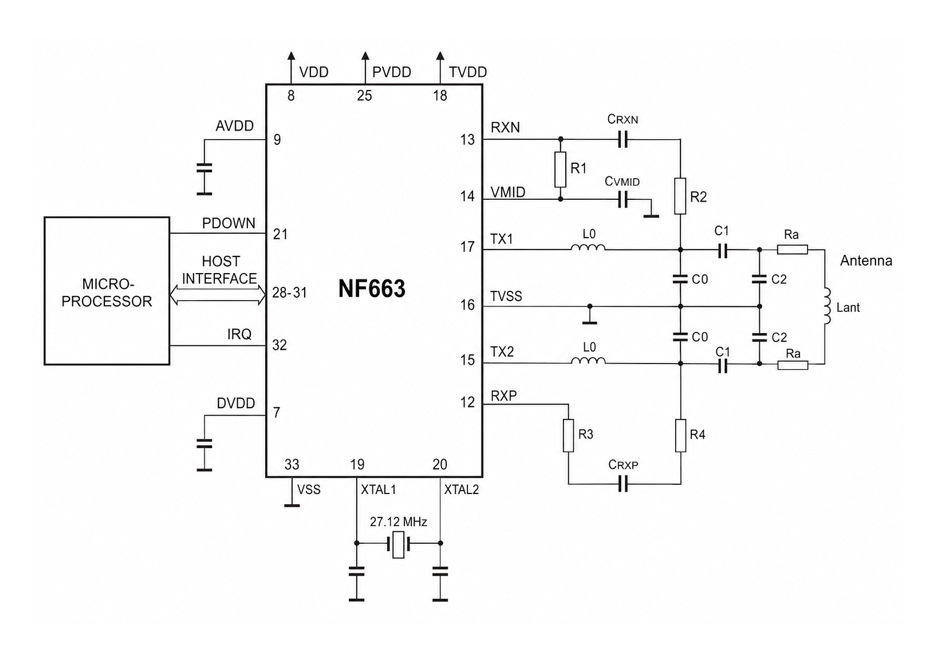
CLRC663 application circuit, explained block by block
The NXP circuit connects the host interface, supplies, oscillator, transmit network and receiver bias. Its architecture is a reference; antenna matching values remain board-specific.
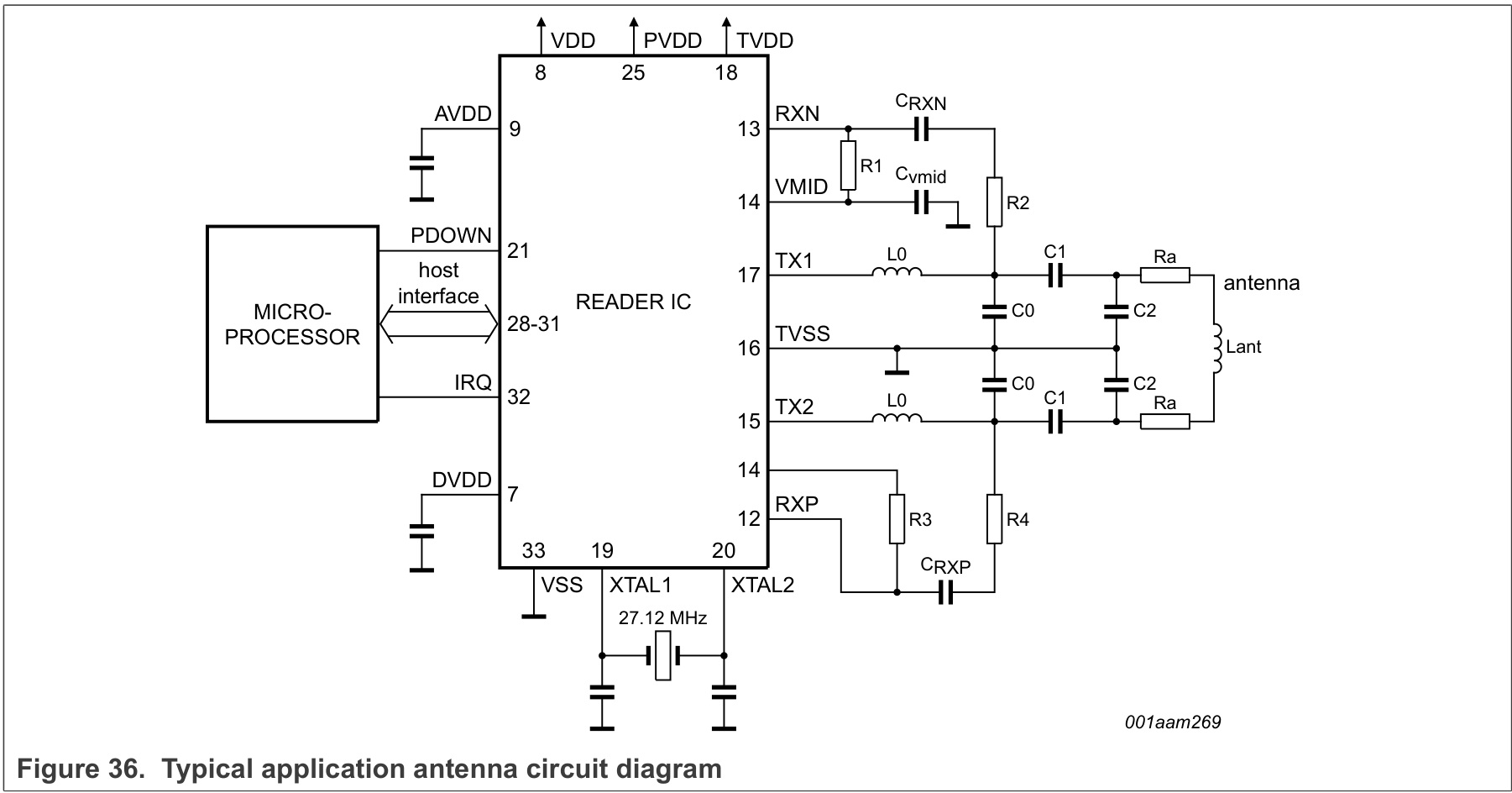 Open full-size JPG ↗
- MCU, IRQ and PDOWNUse the verified host wiring; make command status observable.
- Three external supply inputsCheck the supply map at the IC during field activation.
- 27.12 MHz oscillatorComplete the startup and probing checks before interpreting timeouts.
- Differential transmitterTX1/TX2 feed the RF network; TVSS returns transmitter current.
- EMC low-pass filterL0/C0 suppress harmonics and interact with downstream impedance. Inspect population and routing.
- Antenna matching and dampingSelect matching and damping for the actual coil, enclosure and card population.
- Receiver and VMID referenceCheck receive coupling, scaling and bias separately from field strength.
What read range should you specify for CLRC66303HNY?
Read distance depends on antenna impedance, matching, card type, orientation, supply and enclosure. Measure the assembled RF network before choosing matching and damping values.
- Define the operating region: specify the allowed card distance, lateral offset and angle relative to the finished enclosure.
- Measure successful exchanges: record completed transactions out of attempted transactions, with a latency limit and a defined retry policy.
- Repeat at the design limits: use the required card types, supply and temperature conditions, including nearby metal. Record RF settings and component values with the results.
How do TX1/TX2, RXP/RXN and VMID help locate a fault?
Field present, receive path uncertain
Check RXP/RXN coupling and scaling against the schematic. Use a high-impedance probe under the documented conditions to verify input limits; high antenna voltage can still overload the receiver.
Card detection changes with supply noise
Compare VMID and its return under quiet and field-active conditions using a low-loading probe. Correlated noise warrants checking grounding and coupling before selecting a component change.
Sources: NXP CLRC663, Figure 36 and §14; NXP AN11019 antenna design guide. Related design discussion: CLRC663 antenna design and read-range checks.
Real PCB example: NXP CLEV6630B evaluation board
The real NXP CLEV6630B board pairs CLRC66303 with an LPC1769 over SPI. Its photo shows the reader, power, clock and antenna layout; the reel suffix is unspecified.
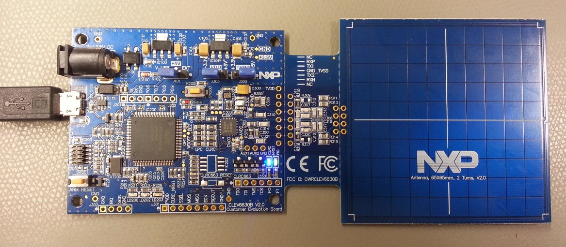 Open full-size JPG ↗
- Power selection
Upper-edge jumpers select the reader rails. Follow the board-specific jumper diagram before applying power.
- Host / interface selection
Inspect the interface straps and host-disconnect paths. An external MCU must not fight the on-board LPC1769.
- Reader crystal region
XT300 is the 27.12 MHz reader crystal in the schematic. XT200 is the separate 12 MHz MCU crystal.
- RF network
The filter, matching and receiver components sit between the reader and antenna connection.
- Antenna area
The supplied antenna is 65 × 65 mm. Its geometry and nearby metal are part of the reference configuration.
Photo: NXP AN11022 Rev. 1.7, Figure 1, © NXP B.V. Numbered overlays identify approximate regions; the original photograph is unchanged.
The reference antenna operates near metal, with default settings tied to its geometry. A different coil can require new matching components and register overrides after LoadProtocol.
Before fabrication: make the failing signals accessible
Check the footprint against the pin map. Provide test access to the supply rails, NSS, SCK, IRQ and PDOWN so the diagnostic sequence can be repeated without disturbing the RF or crystal layout.
Reference-board details: NXP AN11022, §2, Figures 1, 8 and 9.
Public project context: a tag write must become a completed action

In caspar’s prototype, a phone writes an ST25DV04KC tag to wake a battery-powered Pico, which holds power and reads the request over I²C. The useful debugging questions are whether the MCU stays on and when the request can safely be cleared.
A CLRC66303HNY writer is a proposed reader-side extension; it is not the reader used in the published prototype.
Inspect the documented firmware case ↓The NFC field powers the tag-side transaction and wake trigger; the active Pico uses battery power.
Debugging an NFC command that writes successfully but never executes
A successful write response closes only the tag transaction. Read back the request, capture target power and check the application result to locate the missing step. The branches below are a proposed debugging procedure, not measured results from a CLRC663 board.
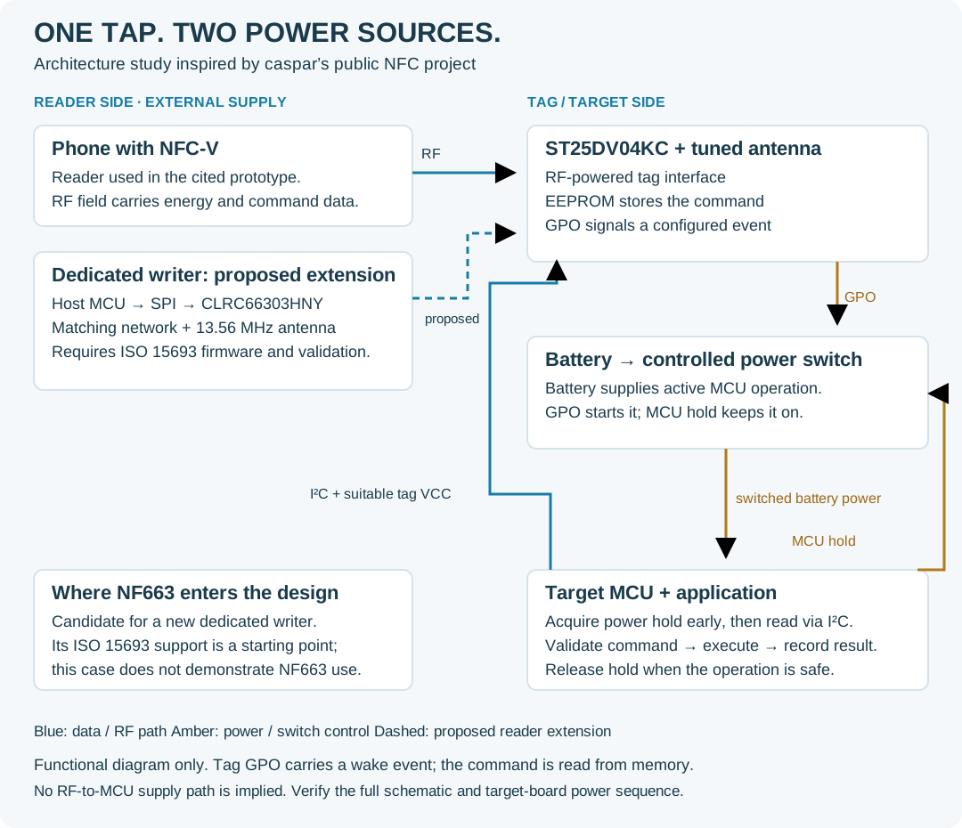 Open scalable architecture diagram ↗
1. Does the stored request match what the reader sent?
For ST25DV04KC, use ISO/IEC 15693 / Type 5 inventory and memory operations. Read back the complete request. If it differs, inspect address, length, write response and interruption timing before debugging the MCU.
If data matches but the MCU rejects it, log the rejection reason: version, length, opcode or integrity check. Define a recoverable record and commit it only after the payload is complete; reject partial writes. Use nonvolatile storage if RF loss must not erase the request. A CRC does not provide authorization.
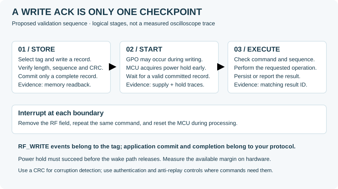 Open scalable checkpoint diagram ↗
2. Does the target wake and remain powered?
Capture GPO, switch control, target supply and hold GPIO together. No wake event: check event configuration and the actual tag write. Wake without supply rise: inspect the power-switch path. Supply rises then collapses: check hold-pin mapping and timing, battery/load behavior and reset. Retest from power-off; the MCU must reach command processing without losing power.
Inspect the public wake/latch schematic and the revision mismatch
 Open original schematic image ↗
Check the revision: the schematic shows GPIO19 for power hold, while the repository README specifies GP28 and describes GPIO19 as unconnected. Verify PCB continuity against the firmware configuration.
The shown R4 = 1 MΩ and C5 = 22 nF give R × C = 22 ms, not a guaranteed boot window. Thresholds, initial gate voltage, leakage and GPO shape affect the usable margin. Measure it; the author’s follow-up explanation describes the early-latch intent.
3. Does execution finish before cleanup or retry?
The ST25DV/Pico prototype provides a concrete implementation and an author-published successful-run example. Its reader is a phone; the handling below is documented in revision 74caa2c.
- Problem addressed
- A partially written request can reach the MCU. Clearing an accepted request while the phone is still reading it can interfere with verification.
- Implemented handling
- Reject invalid/incomplete requests. After applying a valid opcode, mark the request for clearing; perform that clear after RF goes off. See the polling loop.
- Published example
- The log shows opcode
0x11applied as slow LED blinking, followed by RF-off, a successful 16-byte clear and release of the power hold.
One line from the published sample log:
[OK] Cleared request after RF OFF (16 bytes @ 0x01F0, attempts=1, 8ms)The 8 ms value covers the request-clear operation in that example, not RF transfer or boot time. This is author-supplied evidence, not a Nyfea measurement or a before/after reliability benchmark.
Retest the complete action: correlate the accepted request and execution result with a sequence ID. If the result is missing, query status before repeating an action that must not run twice. Test field removal, partial records and duplicate requests; log acceptance, execution and cleanup separately. A pass requires the intended action and matching result, not just a write acknowledgement.
Evaluating NF663: turn the fault checks into project requirements
The same measurement discipline applies when specifying a new writer for sealed-device configuration, e-paper servicing or production tests. Evaluate NF663 on the powered reader side; the prototype’s ST25DV04KC serves the tag side.
Will it communicate with your target?
NF663 supports ISO/IEC 15693 and SPI/I²C/UART. Start with your exact tag and MCU: validate inventory, addressed writes and result readback using NF663-specific software.
Will it recover when a transaction is interrupted?
Define timeouts, retry rules and completion reporting. Test field removal and target resets; do not carry CLRC663 register values into the new driver without checking the NF663 documentation.
Check the specified 3.0–5.5 V supply and −25 to +85 °C limits against the finished product. Qualify the antenna in its enclosure using completed transactions, not field strength alone.
Design references and project support
 Open full-size JPG ↗
 Open full-size JPG ↗
Download the project brief and include the target tag, MCU, antenna/enclosure constraints and available traces. Ask Nyfea for current documentation, samples and the applicable support scope.
Source: NF663 specification. Nyfea supplies NF663; the proposed writer uses are not demonstrated implementations of the cited prototype.