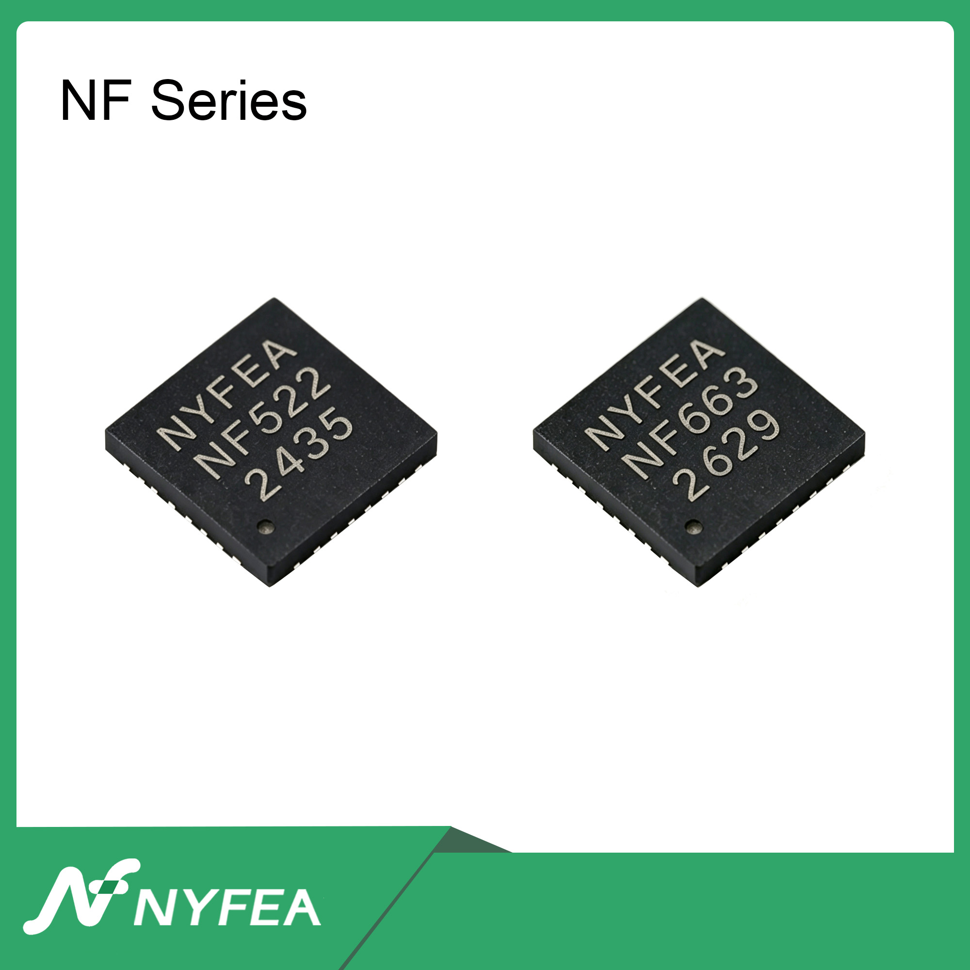
NF663 Reader Board Bring-Up: From SPI Communication to Reliable Card Detection
A layer-by-layer engineering guide for debugging an NF663 13.56 MHz RFID reader board when register access works but cards are not detected reliably.
DIRECT ANSWER
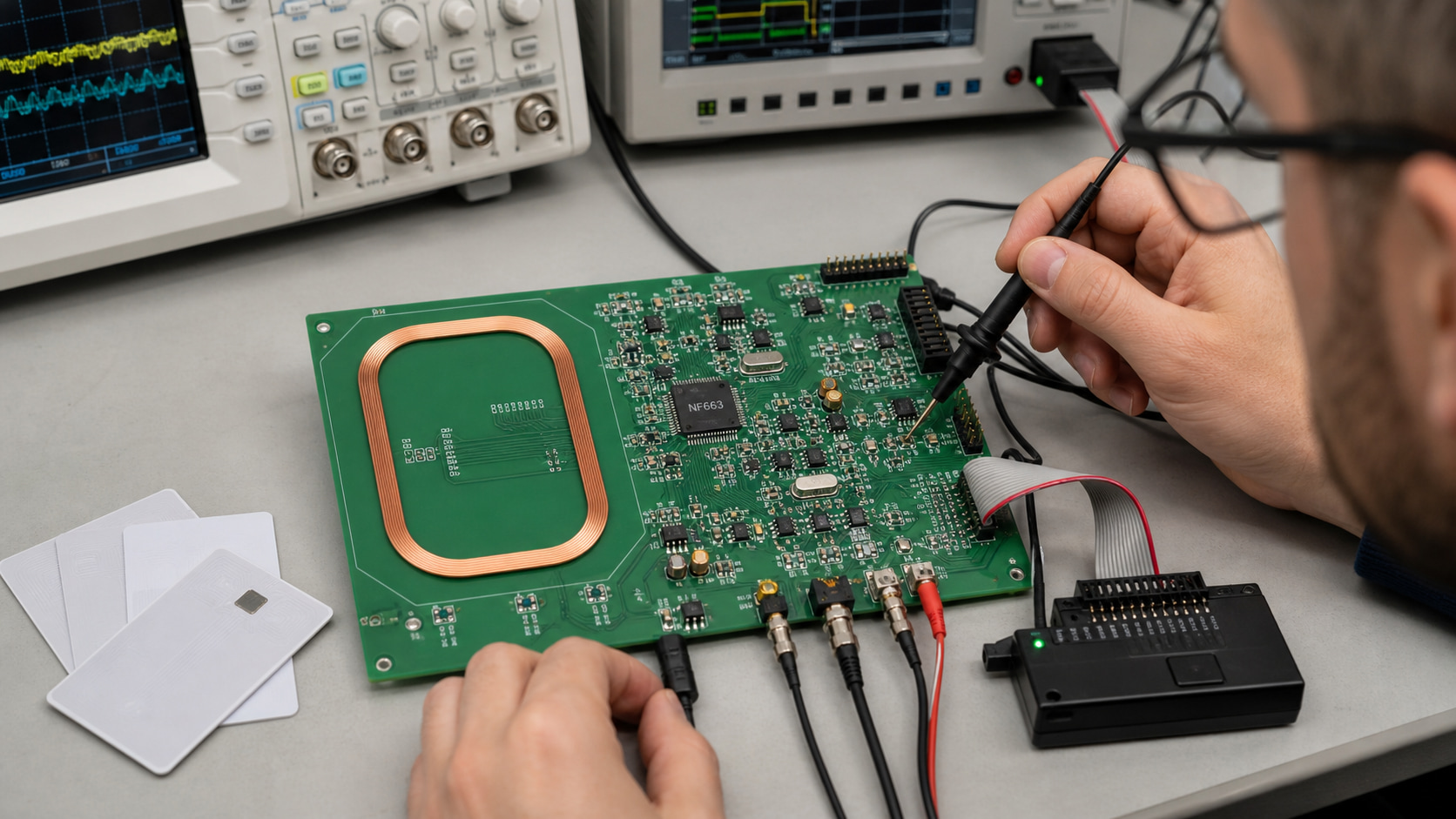
If an MCU can read NF663 registers but no card is detected, do not immediately change antenna capacitors or rewrite the complete protocol stack. First prove stable power, reset and the 27.12 MHz clock; then prove repeatable SPI read/write behavior; next verify command completion, interrupt status, timer operation and FIFO length; only after those layers pass should you diagnose the 13.56 MHz field, matching network, receiver configuration and card protocol. A carrier visible on TX1/TX2 confirms activity at the transmitter pins, but it does not prove that sufficient magnetic field reaches the card or that the reader can demodulate the card response.
A frequent first-board failure looks deceptively encouraging. The host MCU starts, SPI traffic is visible, NF663 registers return plausible values and TX1/TX2 show a periodic waveform. Yet an ISO/IEC 14443 Type A card is detected only occasionally, an ISO/IEC 15693 label never answers, or the polling loop ends in a timeout every time.
This guide follows that failure pattern from the connector to the antenna. The objective is not to present a universal register script. It is to show the measurement order that prevents an engineer from spending hours tuning the wrong layer of the system.
1. The symptom: SPI works, but the reader does not see a card
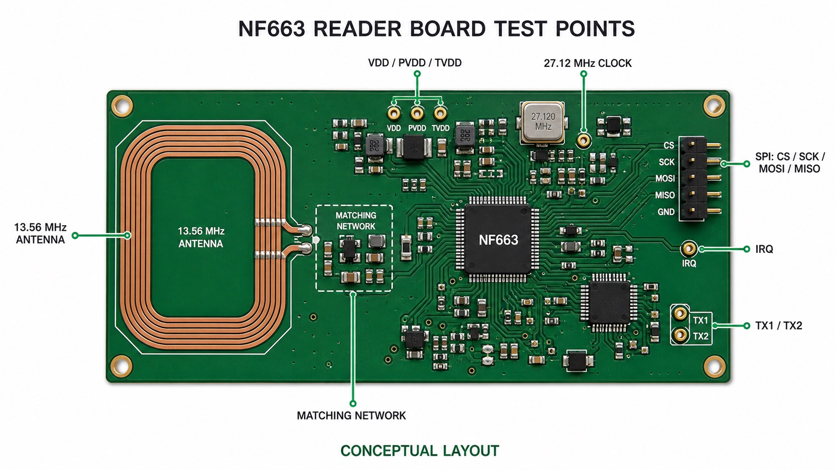
The prototype contains an NF663 reader IC, a host MCU, a 27.12 MHz crystal, separate logic and transmitter supply paths, SPI, IRQ, an EMC filter, an impedance-matching network and a rectangular loop antenna. The first firmware can read and write registers, but the application reports “no card” for every polling attempt.
What a successful SPI transaction proves
- The MCU can assert chip select and exchange bits with the selected interface.
- At least part of the NF663 digital supply and host interface is active.
- The firmware is not completely disconnected from the reader IC.
What it does not prove
- That the transmitter supply and RF driver are operating correctly.
- That a command starts, completes and produces the expected interrupt.
- That FIFO length and receive data are interpreted correctly.
- That the matching network delivers useful field strength to the antenna.
- That the configured protocol matches the presented card or tag.
Evidence boundary: this is a diagnostic workflow example, not a customer-specific measured case study. Register addresses and electrical reference conditions below are tied to the controlled NF663 technical specification; final component values and pass limits must be established on the actual PCB and enclosure.
2. Layer 1 — prove power, reset and clock before debugging firmware
Begin with static hardware conditions. Measure every NF663 supply at the device, not only at the regulator. The transmitter supply can experience a different drop and ripple profile from the digital rail when the RF field is enabled. Record the no-field and field-on values so later antenna changes are not confused with a power-integrity problem.
- Power rails: verify VDD, PVDD and TVDD against the controlled NF663 specification and confirm that RF activation does not pull a rail outside its intended operating range.
- Reset: confirm the reset pin reaches valid logic levels and is released only after the required supplies and clock conditions are ready.
- Clock: verify stable operation of the 27.12 MHz crystal circuit. Use a low-capacitance probe or a buffered clock output where available; an ordinary probe can disturb the oscillator.
- Interface selection: confirm that board straps and firmware agree on SPI rather than I²C or UART.
- Grounding: check exposed-pad soldering, return paths and continuity between the NF663 ground domain, matching network and antenna reference structure.
Decision: if a rail collapses, reset chatters or the clock is absent, stop. Register reads obtained under marginal conditions are not a reliable foundation for RF debugging.
Do not drive internal buffer nodes. DVDD, AVDD and VMID are intended only for their specified buffer capacitors. Applying an external supply to these pins may damage the device. Validate VDD, PVDD and TVDD as the external supply paths and follow the current NF663 pin description for capacitor placement.
3. Layer 2 — make the SPI interface demonstrably repeatable
One successful read is insufficient. Capture a short, deterministic start-up test with a logic analyzer. Read several stable registers repeatedly, write a reversible configuration value, read it back and restore it. Compare the decoded bytes with the waveform to catch bit-order, clock-phase, chip-select and bus-release errors.
| Observation | Likely layer | Next check |
|---|---|---|
| MISO remains 0x00 | Power, reset, interface selection or a held-low bus | Measure the pin, isolate other SPI devices and confirm the selected interface. |
| MISO remains 0xFF | Open bus, inactive device or missing chip select | Check continuity, CS timing, reset release and MCU pin direction. |
| Values change between identical reads | Signal integrity, timing or unstable power/clock | Lower SCK, inspect edges and confirm decoupling at NF663. |
| Readback is stable but the command times out | Command, IRQ, timer, protocol or RF layer | Move to the state-machine checks; do not replace SPI wiring. |
If NF663 shares the bus with flash memory, a display or an SD card, verify that every non-selected device releases MISO. A reader can appear healthy in a minimal test and fail only after another peripheral is initialized.
4. Layer 3 — debug the command, interrupt and FIFO as one transaction
The next checkpoint is not “did IRQ become high?” It is whether the complete transaction has a coherent start, event and result. Before issuing a polling command, clear stale interrupt flags, enable the required sources, configure the timeout path and record the starting FIFO state. After the event or timeout, read the relevant status together with FIFO length.
- Apply the intended protocol configuration for a known-good card.
- Clear previous interrupt events and flush stale FIFO data.
- Enable the required receive, error and timer-related interrupt sources.
- Start the command and record the exact start time.
- Capture the physical IRQ pin and the SPI read of interrupt status.
- Read error/status information and FIFO length before consuming payload bytes.
- Classify the result as command-not-started, timed-out, receive-error or valid response.
Important: an interrupt register value alone is not the card response. Interrupt bits describe events. Response bytes, when present, belong in the FIFO and must be interpreted with the corresponding status and error conditions.
If the physical IRQ pin never changes but status bits do, check IRQ polarity, output configuration and the MCU’s edge selection. If neither changes, verify that the command was accepted and that the timer or receive path was actually started.
NF663 register checkpoints for a reproducible trace
Capture a compact register trace at command start, IRQ or timeout, and before FIFO data is consumed. The addresses below identify useful checkpoints; they are not a universal configuration script or a set of guaranteed values.
| Checkpoint | NF663 register | Bring-up evidence |
|---|---|---|
| Command state | Command (00h) | Confirms which command the reader is expected to execute at the captured point. |
| FIFO state | FIFOControl (02h), FIFOLength (04h) | Shows whether stale data was flushed and whether a response produced bytes. |
| Event source | IRQ0 (06h), IRQ1 (07h) | Separates receive, timer and other events from the physical IRQ-pin observation. |
| Error and status | Error (0Ah), Status (0Bh) | Provides context for an empty FIFO, timeout or invalid response. |
| RF driver setup | DrvMode (28h), TxAmp (29h), TxCon (2Ah), TxI (2Bh) | Records the active transmitter configuration before analog measurements are compared. |
| Device identification | Version (7Fh) | Adds a stable identification checkpoint to startup logs and board-to-board comparisons. |
5. Layer 4 — a 13.56 MHz waveform does not prove a working RF link
After the digital transaction is repeatable, inspect the RF system. A correct carrier frequency at TX1/TX2 only proves that the driver is switching. Card operation depends on the current delivered through the EMC filter and matching network, magnetic coupling to the tag, modulation of the outgoing field and recovery of the much smaller load-modulated response.
- Use a differential probe or the measurement method specified for the reader frontend. Do not short one side of a differential RF output with an earth-referenced probe ground.
- Use a small field probe to confirm that the antenna, not merely the IC pin, produces a magnetic field.
- Inspect component population, capacitor dielectric, inductor loss and solder joints in the EMC and matching networks.
- Measure antenna impedance or resonance on the assembled PCB and in the intended enclosure. Calculated values are only starting values.
- Check the receive path and protocol-specific analog settings before increasing transmitter strength.
A common failure pattern is a clean-looking carrier at the device pins and an extremely weak field at the loop. That points toward an open antenna path, a badly mismatched network, the wrong component values or excessive loss—not toward a new SPI driver.
Reference condition, not a universal antenna target. The NF663 quick-reference typical TVDD-current condition uses the complementary driver with an antenna matched to 40 Ω between TX1 and TX2 at 13.56 MHz. Treat this as a datasheet test condition—not as a guaranteed antenna impedance, read range or production matching target.
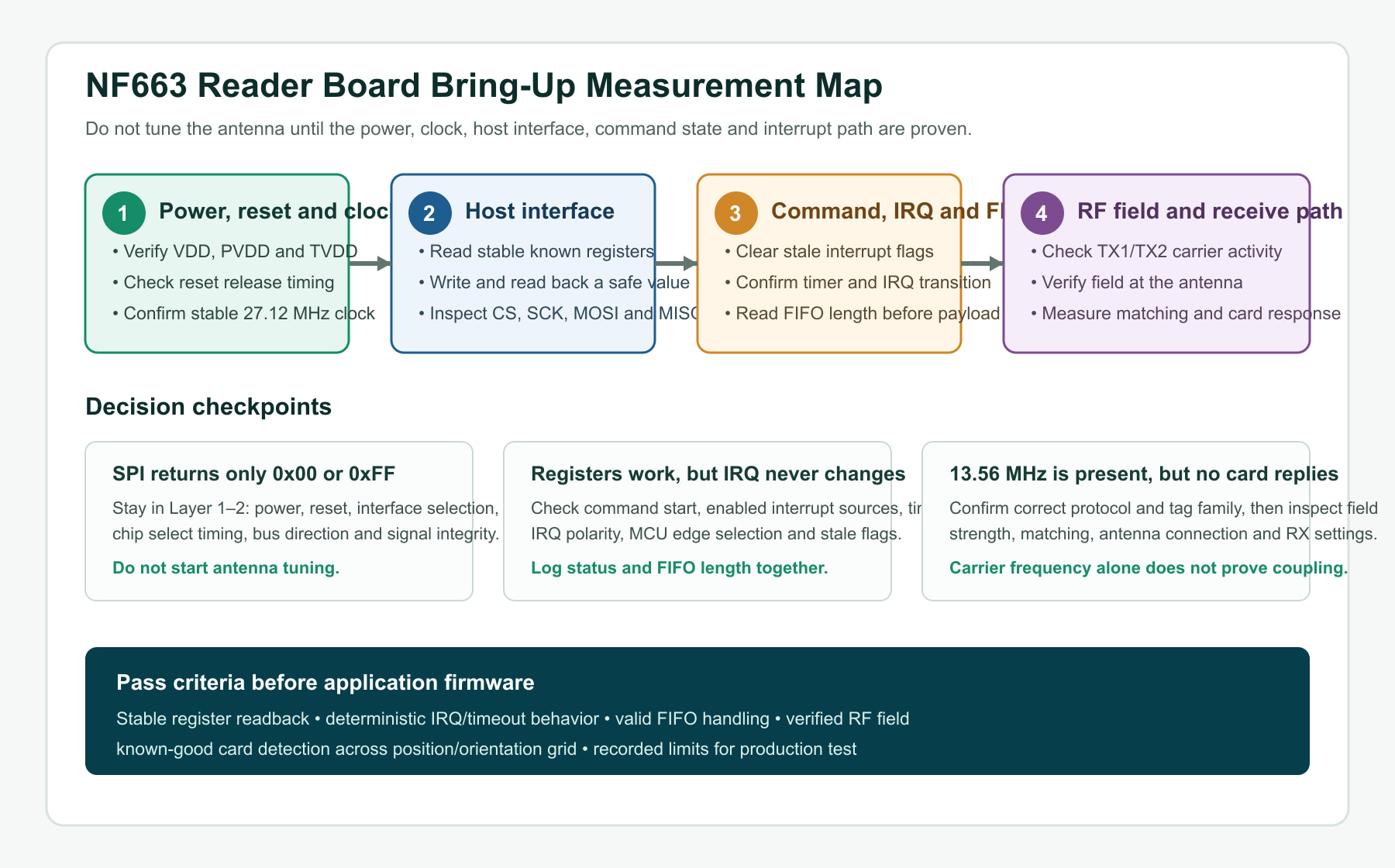
6. Verify the card technology before changing hardware
Use at least one known-good credential for each required protocol. A 125 kHz key fob cannot be detected by a 13.56 MHz reader, and two objects with similar plastic housings may use different air interfaces. Within 13.56 MHz, an ISO/IEC 14443 Type A configuration is not an ISO/IEC 15693 inventory sequence.
For the first successful exchange, reduce variables: use one card, place it parallel to and centered over the loop, keep a repeatable gap and start with a protocol configuration already validated for that card family. Only then expand the position, orientation and tag set.
7. Diagnostic workflow example: from “no card” to a stable UID read
In this representative bring-up, register readback remained stable at several SPI clock rates. The clock and supplies were valid, and IRQ changed when a timer expired. TX1/TX2 showed carrier activity, but a field probe over the antenna produced a much lower signal than the reference board.
Inspection found that two matching capacitors had been populated from an early BOM revision. After the intended values were installed, the assembled antenna was measured and the network was adjusted for the actual PCB. Field strength increased, the receive interrupt occurred and FIFO length became non-zero. The firmware then returned a stable UID from the known-good Type A card.
The key lesson is diagnostic separation: SPI had never been the root cause. The useful evidence was the combination of stable register access, deterministic timer/IRQ behavior, weak antenna field and empty receive FIFO.
8. Minimum instrumentation and what each tool proves
| Tool | Use during bring-up | What it cannot prove alone |
|---|---|---|
| Digital multimeter | Rail voltage, reset level, continuity and static faults | Clock integrity, RF waveform or short transients |
| Oscilloscope | Clock, reset, IRQ, supply ripple and RF activity with correct probes | Antenna impedance or protocol correctness |
| Logic analyzer | SPI transaction order, timing and MCU/IRQ correlation | RF field strength or analog receive margin |
| Near-field probe | Relative field presence and board-to-board comparison | Standards compliance or precise matching impedance |
| VNA or impedance analyzer | Antenna and matching behavior in the assembled environment | Firmware state, IRQ handling or FIFO parsing |
| Known-good card set | Protocol, position and orientation validation | Complete interoperability or production coverage |
9. Production-ready diagnostic hooks
Bring-up measurements should become production diagnostics rather than disappearing after the first prototype works. Reserve test access for critical rails, reset, clock observation, SPI, IRQ and RF comparison. Firmware should be able to report a compact diagnostic record without exposing secret application data.
- NF663 reset completed and stable registers read
- Selected host interface confirmed
- Expected clock source active
- Interrupt line toggles during a controlled timer test
- FIFO flush, length and overflow handling verified
- RF field-on current within the approved board window
- Known-good Type A and/or ISO/IEC 15693 card detected
- Position and orientation grid meets the product requirement
- Timeout recovery succeeds without a power cycle
- Shared SPI peripherals cannot hold MISO active
10. NF663 bring-up acceptance criteria
Do not define success as a single card read on an open bench. Record repeatable limits that can be compared between boards and firmware versions:
- Stable register readback after cold start, warm reset and repeated sleep/wake cycles.
- Deterministic command completion, timeout and error recovery.
- Valid IRQ and FIFO behavior under rapid card presentation and card removal.
- Read-zone coverage across the intended card positions and orientations.
- Performance with the production enclosure, display, battery, cables and nearby electronics active.
- Results across the actual card/tag set, not one convenient laboratory sample.
Engineering FAQs
Why can SPI communication work while NF663 still cannot detect a card?
SPI only proves host access to the digital interface. Card detection additionally requires a valid command sequence, interrupt and timer behavior, correct FIFO handling, an active RF driver, a matched antenna, a usable receive path and a protocol that matches the presented credential.
What should I measure first on a new NF663 board?
Start with the NF663 supply rails at the device, reset timing and the 27.12 MHz clock. Then prove repeatable register access. This order prevents an unstable hardware foundation from being misdiagnosed as a protocol or antenna problem.
TX1 and TX2 show 13.56 MHz. Why is there still no card response?
The driver may be switching while little useful energy reaches the antenna. Check the EMC filter, matching components, antenna connection, field at the loop, receiver configuration and the actual card protocol. Frequency alone does not establish field strength or receive sensitivity.
Why does one card work while another card or key fob does not?
Confirm frequency and protocol first. A 125 kHz credential is incompatible with a 13.56 MHz reader. Even within 13.56 MHz, Type A, Type B and ISO/IEC 15693 require different polling and framing. Card size, antenna orientation and loading also change coupling.
How do I separate a firmware fault from an antenna fault?
Use layer checkpoints. If registers are unstable, stay at power and SPI. If timer interrupts and FIFO operations are deterministic but the field probe is weak or no receive event occurs, move to the RF path. Compare against a known-good board using the same firmware and credential.
Can CLRC663 example code be used directly with NF663?
CLRC663 documentation can provide useful architectural and debugging concepts for engineers familiar with multi-protocol 13.56 MHz frontends. It should not be treated as proof of register, timing, firmware or analog-setting compatibility. Port and validate the design against the current NF663 controlled documentation.
Does one successful UID read mean the design is production-ready?
No. Production readiness requires repeatable cold starts, timeout recovery, card removal behavior, an approved card set, position and orientation coverage, enclosure testing and defined manufacturing limits for power, RF and digital diagnostics.
Download the NF663 technical specification
The controlled NF663 document should remain the authority for pin functions, electrical limits, commands, registers and protocol settings. Use this article as a bring-up method, not as a replacement for the product specification.
Download NF663 Technical Specification (PDF)
Need help reviewing an NF663 prototype?
Share the intended card protocols, host interface, antenna dimensions, enclosure constraints and measured failure layer with NYFEA. A useful review starts with evidence from power, clock, SPI, IRQ/FIFO and RF—not with read range alone.