MFRC52202HN1 vs NF522: SPI, Antenna & D99 Read-Range Test Guide
This MFRC52202HN1 replacement test guide defines a controlled method for assessing NYFEA NF522 through SPI reliability, 13.56 MHz antenna tuning and D99 read-range validation—without treating shared headline features as proof of pin, register, firmware or RF compatibility.
DIRECT ANSWER
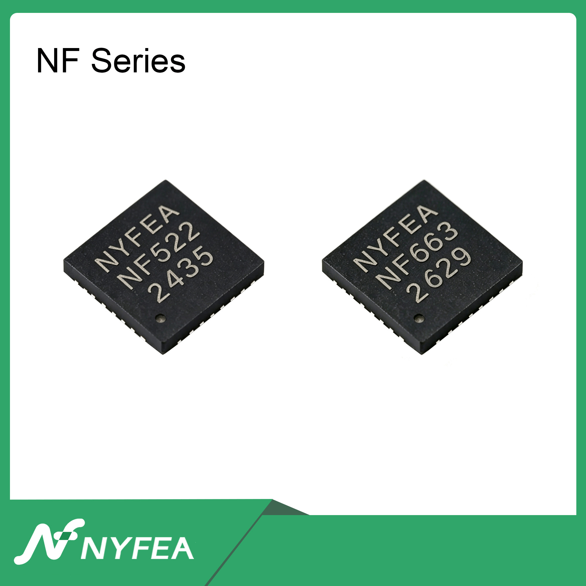
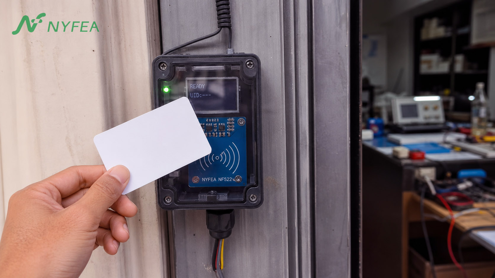
NYFEA NF522 can be evaluated as an independent 13.56 MHz reader-IC candidate for a new or redesigned product that previously used MFRC52202HN1, but it must not be presented as a drop-in replacement without design-specific evidence. The two devices share SPI, I²C and UART host options, a 64-byte FIFO and a 27.12 MHz crystal connection. Those similarities do not establish package, pin, electrical, register, initialization, firmware or antenna-network compatibility.
The defensible evaluation sequence is: prove power, clock, reset and host communication; test SPI integrity under a defined workload; tune each assembled RF network independently; then compare stable read range with the same Type A cards, geometry, environment and acceptance rule. This article defines that method and deliberately does not invent unpublished test results.
CONTENT UPDATE · AUGUST 29, 2026
What changed in this MFRC52202HN1-to-NF522 test guide?
- The guide now separates documented device capabilities from design-specific compatibility conclusions.
- The read-range section defines D99 with a one-sided 95% exact-binomial lower confidence bound instead of relying on a single successful read.
- The reporting table labels all unavailable measurements as pending, so a proposed qualification method cannot be mistaken for completed test evidence.
60-SECOND ENGINEERING VERDICT
What can be reused—and what must be revalidated?
NF522 is a redesign candidate for an MFRC52202HN1-based product, not a compatibility claim. Preserve the released product requirements and application behavior; re-establish every device-specific electrical, firmware and RF assumption.
| Engineering question | Short answer | Required evidence |
|---|---|---|
| Can NF522 be soldered onto the existing footprint? | Do not assume so from QFN32 or 13.56 MHz alone. | Controlled package drawing, exposed-pad requirements and a complete pin-by-pin audit. |
| Can the existing firmware be reused? | The application layer may be reusable; the low-level device adapter must be independently verified. | Reset, identification, register, FIFO, IRQ, timeout and recovery transaction captures. |
| Can the antenna be reused? | Geometry may be a starting point; the matching BOM is not automatically transferable. | Measured and retuned network on the NF522 PCB in the final mechanical assembly. |
| What supports a release decision? | Passing digital, RF and application-level limits under declared conditions. | Traceable SPI results, antenna records, D99 confidence limits, environmental margin and fault recovery. |
1. Decision boundary: alternative evaluation, not an automatic replacement
NXP currently identifies ordering code MFRC52202HN1 as End of Life and not recommended for new designs, and names CLRC663 plus as its recommended NXP product for new designs. NF522 is a separate NYFEA device and an independent engineering candidate; it is not an NXP-endorsed successor.
The correct migration question is therefore not “Do the two part numbers look similar?” It is “Can an NF522-based board meet the released product requirements after its pins, rails, host transactions, firmware, RF network and complete read zone have been re-established?”
2. Documented functional baseline
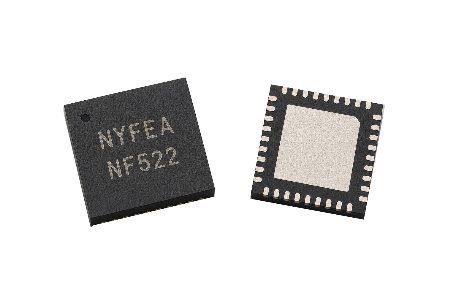
The table below separates public device capabilities from migration conclusions. “Same” or “higher” headline values never replace a pin-by-pin and transaction-by-transaction review.
| Item | MFRC52202HN1 documented baseline | NF522 documented baseline | Evaluation meaning |
|---|---|---|---|
| Carrier | 13.56 MHz | 13.56 MHz | A common carrier does not establish RF-network compatibility. |
| Reader protocols | ISO/IEC 14443 Type A, MIFARE and NTAG | ISO/IEC 14443 Type A, Type B and ISO/IEC 15693 reader modes | Use Type A cards for the common A/B comparison. Test NF522-only protocol coverage separately. |
| SPI | Up to 10 Mbit/s | Up to 12 Mbit/s; modes 0 and 3 are listed | Compare both devices at common rates up to 10 Mbit/s. Treat 12 Mbit/s as an NF522-only test. |
| I²C | Fast mode to 400 kBd and High-speed mode to 3.4 Mbit/s | Up to 400 kbit/s | An MFRC522 High-speed-mode implementation requires redesign. |
| UART | Up to 1228.8 kBd | Up to 1.2288 Mbit/s | Still verify reset defaults, framing, register access and I/O levels. |
| FIFO | 64-byte transmit/receive FIFO | 64-byte transmit/receive FIFO | Capacity does not establish identical FIFO flags, thresholds or error behavior. |
| Clock | 27.12 MHz crystal connection | 27.12 MHz crystal connection | Measure startup, loading and PCB parasitics on each board. |
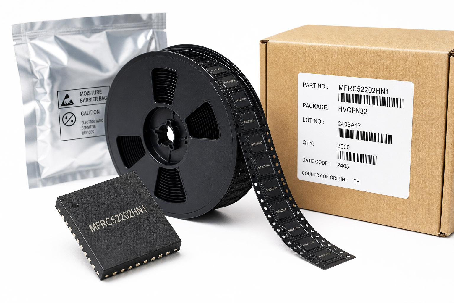
| Package | HVQFN32, SOT617-1 | QFN32 | Pin count alone is not a footprint or pin-map statement. |
| Published range statement | Typical read/write distance up to 50 mm, dependent on antenna size and tuning | Product-data statement up to 100 mm, dependent on antenna and system conditions | The two “up to” values are not a controlled comparison and must not be used as one. |
Comparison rule: retain product requirements, target cards, read-zone fixtures, fault policy and traceability. Re-establish the footprint, power tree, low-level driver, matching network and measured performance limits.
3. Build a controlled comparator
Use two dedicated boards rather than adapting one device onto the other device's pads with long wires. Keep the test controller, log format, power source, cable construction and application sequence common, while allowing each reader IC to use its own correct pin map, decoupling, reset circuit and matching network.
- Freeze the MFRC52202HN1 baseline. Archive the schematic, PCB revision, antenna geometry, matching BOM, firmware commit, approved cards, enclosure and measured read zone.
- Build an NF522-specific board and driver. Do not hide unverified register assumptions behind a common part-number alias.
- Reuse a common test controller. Keep the card transaction, logging and acceptance logic above device-specific driver adapters.
- Use the same Type A comparator cards. Type B and ISO/IEC 15693 are NF522 extension tests, not MFRC52202HN1 comparison points.
- Tune each RF network independently. Retaining antenna geometry as a starting point is reasonable; copying matching values without measurement is not.
Recommended software boundary
Test controller, logger and acceptance rules
                    │
             Common reader API
               ┌────┴────┐
               │         │
       MFRC522 adapter  NF522 adapter
       register map A   register map B
This structure makes a fair application-level comparison possible while preserving separate commands, registers, initialization, IRQ and recovery behavior.
4. Prove power, clock, reset and device access first
Do not begin with read range. An RF result is uninterpretable until the digital foundation is known to be stable.
- Capture every supply rail during ramp, reset release, initialization and RF-field activation.
- Confirm the 27.12 MHz clock starts and remains stable under the released loading condition.
- Verify reset width, interface-selection straps and the first host transaction.
- Read the device-identification or version information defined by the relevant controlled data.
- Exercise FIFO clear, write, readback, boundary and recovery behavior.
- Run the device-supported internal self-test before enabling the RF field.
In the widely used open-source MFRC522 library, VersionReg values 0x91 and 0x92 are associated with MFRC522 versions 1.0 and 2.0. Field reports commonly associate 0x00 or 0xFF with power, wiring, chip-select, reset or host-communication faults. A valid 0x92 read proves digital access and version identification; it does not prove that the transmitter, receiver, matching network or antenna is working.
5. SPI reliability test
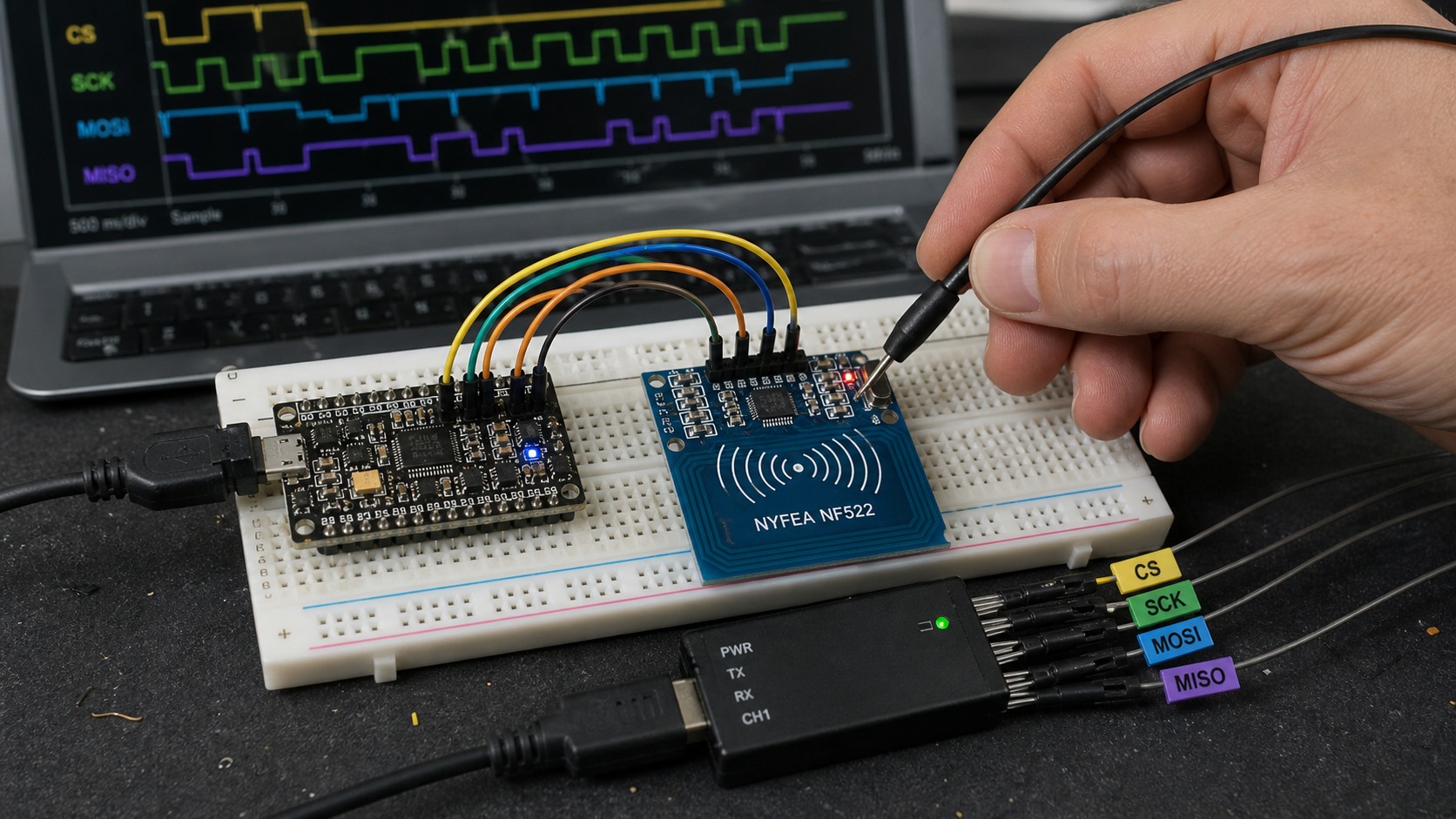
Compare both devices at common SPI clock rates of 1, 2, 5, 8 and 10 MHz. Test NF522 at 12 MHz separately. The proposed workload below is a qualification starting point, not a claim that these cycles have already been completed:
- 100,000 register write/readback operations at each clock rate;
- 10,000 complete 64-byte FIFO fill and verification cycles;
- 10,000 reset, initialization and identity-confirmation cycles;
- an extended run that records every timeout, retry, reset and power-cycle recovery.
Do not reduce the result to “pass” or “fail.” Classify readback mismatch, stuck-high or stuck-low MISO, timeout, FIFO-length error, missing IRQ, recovery after clock reduction, recovery after reset and recovery requiring a power cycle.
A reasonable minimum gate is zero unrecovered bus lockups within the declared workload. Whether a recovered retry is acceptable depends on the end product's availability and safety requirements and must be defined before the run.
6. Antenna and matching-network validation
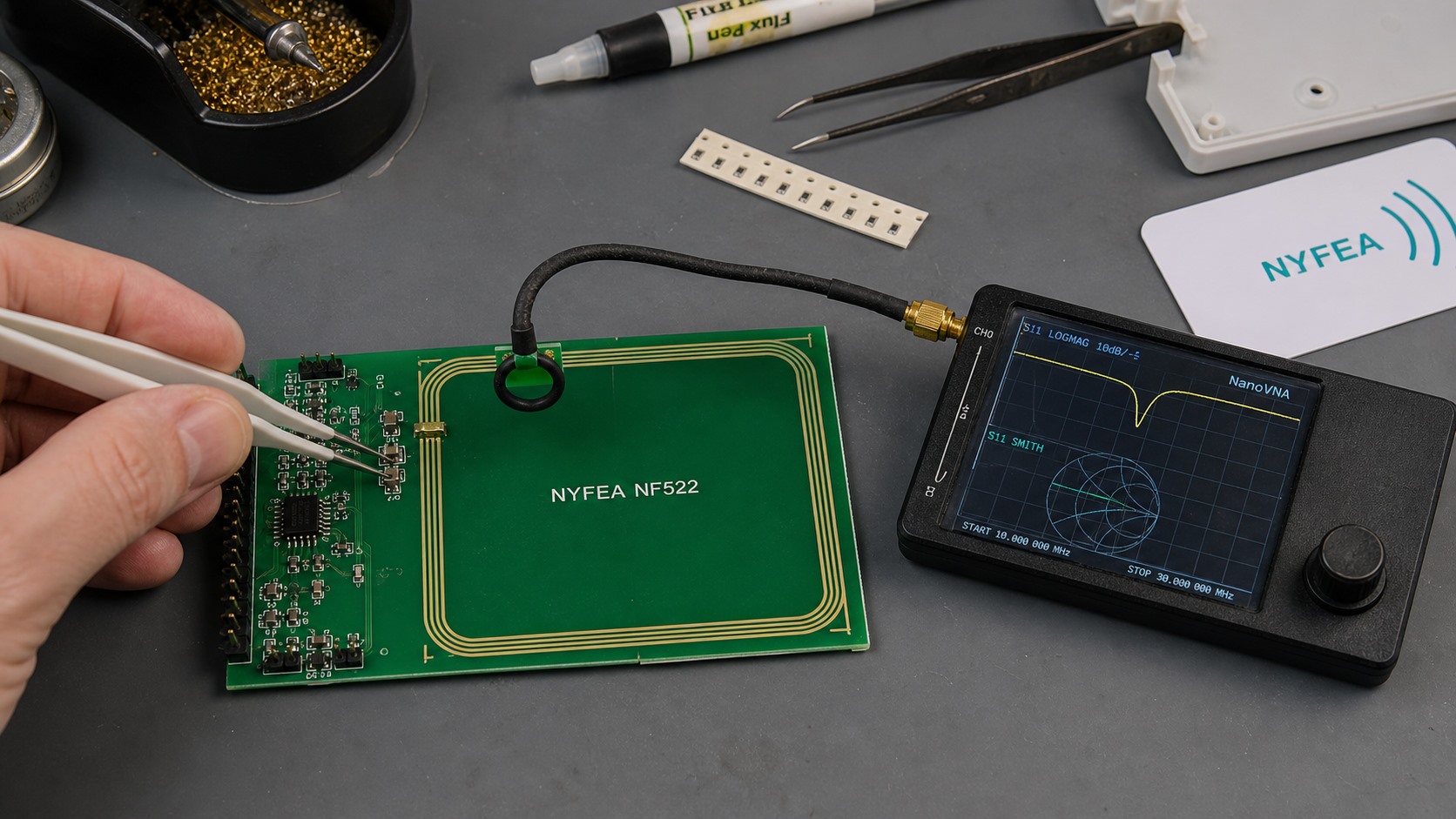
Record the antenna geometry, inductance, resonance, quality factor, matching response, TX waveform, receive-path condition and component revision. Repeat the measurement after installing the intended enclosure, battery, display, shield, cables and any nearby metal.
A VNA result is meaningful only when its fixture, calibration reference and coupling method are recorded. A long uncalibrated lead can change the network being measured. Keep fixture loading consistent between board revisions and archive the raw sweep rather than only a screenshot.
Receiver gain is not transmitter power. In common MFRC522 software, PCD_SetAntennaGain() changes the RFCfgReg receiver-gain field. Maximum receive gain can amplify interference as well as a card response; it must be logged as a controlled variable, not treated as an automatic range upgrade.
7. Define stable read range as D99
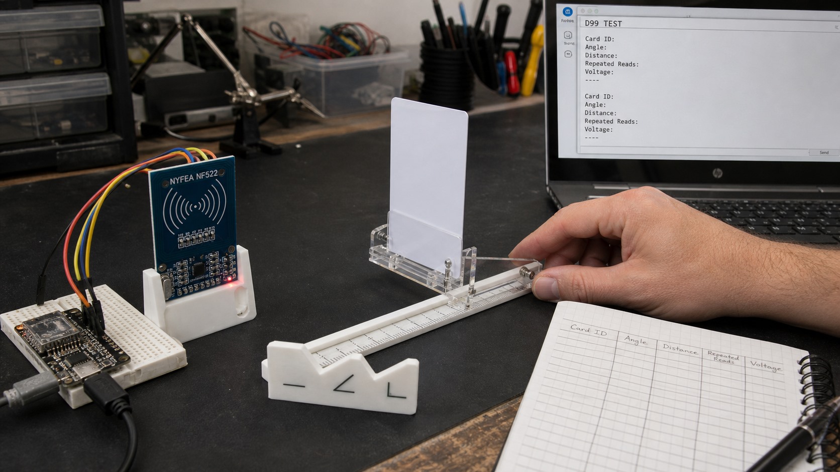
Data-sheet statements such as “up to 50 mm” and “up to 100 mm” are not directly comparable when the antenna, card, matching, supply, enclosure and success criterion differ. An observed 99% result is also not the same as statistically demonstrating that the underlying success probability is at least 99%. Use a shared definition:
Report both the observed rate and its confidence bound. For example, 990 successful transactions out of 1,000 is an observed 99% rate, but its one-sided 95% lower bound is below 99% and therefore does not pass this D99 rule. A 1,000-of-1,000 result has a lower bound of approximately 99.70%; the test report must still state the sample size, confidence method and all exclusions.
Define one transaction before testing. A discovery-range transaction may require REQA, anticollision and Select within a fixed deadline. An application-range transaction may additionally require authentication and a declared block read. Count a timeout, CRC/protocol error, hidden retry or reset recovery according to a policy written before the run; do not redefine success after seeing the data.
At each point, record at least the card identity, distance, 0°/45°/90° orientation, supply voltage, temperature, RF configuration, receiver gain, transaction profile, number of attempts, successes, timeouts, CRC/protocol errors, retries and response-time distribution. A practical screening starting point is 1,000 transactions per card, point and orientation, but the confidence rule—not a round sample count—controls the conclusion.
Use only card technologies supported by both devices for the common comparison. NF522 Type B and ISO/IEC 15693 performance belongs in a separate extension test.
8. Use a staged test plan, not one oversized headline number
A credible program separates fast fault discovery from design qualification and production guardbanding. The quantities below are planning examples, not universal certification limits; product risk, failure cost and regulatory obligations determine the final sample plan.
| Stage | Purpose | Example starting scope | Decision |
|---|---|---|---|
| A — Engineering screening | Expose wiring, reset, driver, card-technology and gross RF faults quickly. | At least three samples per device, representative Type A cards, key SPI rates, three orientations and focused distance points. | Allows the design to enter controlled tuning; it is not a release result. |
| B — Design qualification | Quantify digital reliability, D99, timing, voltage, temperature and mechanical sensitivity. | Multiple samples and lots, approved card set, final antenna and enclosure, declared transaction profile and confidence rule. | Supports a design-level migration decision when every predeclared limit passes. |
| C — Production guardband | Verify lot variation, manufacturing tolerance, recovery behavior and ongoing process margin. | Risk-based lot sampling, controlled production fixtures, golden-unit correlation and retained raw records. | Supports production control; it does not replace end-product compliance work. |
The final report must publish the actual sample count, lot count, board revision, card set, exclusions, failures and raw-record summary. Never present a proposed matrix as completed test evidence.
| Evidence group | Record required | Why it matters |
|---|---|---|
| Hardware | Board revision, IC sample and lot, BOM, antenna geometry, enclosure | Prevents a result from being detached from the unit that produced it. |
| Firmware | Commit, driver adapter, initialization values, gain and retry policy | Separates silicon behavior from software configuration. |
| Instruments | Model, calibration status, fixture and connection point | Makes SPI and RF measurements reproducible. |
| Cards | Technology, identifier, supplier, lot, size and orientation | Card coupling and protocol support materially affect range. |
| Environment | Voltage, temperature, noise sources and mechanical stack | Open-bench success does not define final-product margin. |
9. Publish measured results without hiding the evidence boundary
The table below is intentionally unpopulated. Replace every pending field only with traceable records from the declared board, sample, card and test method. Until then, the page is a validation protocol—not a test-results report.
| Metric | MFRC52202HN1 | NF522 | Release interpretation |
|---|---|---|---|
| 10 MHz SPI transactions | Pending measured record | Pending measured record | Declare total operations, errors, retries and unrecovered faults. |
| 64-byte FIFO verification errors | Pending measured record | Pending measured record | Identify pattern, frequency, clock and recovery path. |
| Reset/initialization failures | Pending measured record | Pending measured record | Separate reset, clock, bus and device-state failures. |
| Type A D99 at 0° | Pending measured record | Pending measured record | State card, antenna, gain, voltage and environment. |
| Type A D99 at 45° and 90° | Pending measured record | Pending measured record | Report the read-zone shape, not only the best axis. |
| P95/P99 transaction time | Pending measured record | Pending measured record | Include timeout and retry policy. |
| Temperature and voltage shift | Pending measured record | Pending measured record | Compare against the released product limits. |
10. Conditions for an NF522 migration decision
An NF522 prototype may advance only when the following evidence is complete:
- the schematic and footprint have been reviewed against the controlled NF522 documentation;
- firmware uses an NF522-specific register map and initialization sequence;
- SPI, reset, IRQ, timeout and recovery tests meet declared limits;
- the antenna network has been measured and retuned in the final PCB and enclosure;
- D99 and orientation results meet the product requirement for every approved card;
- power, temperature, interference, EMC and lot variation have been evaluated;
- security, regulatory and system-certification obligations are closed at end-product level;
- procurement, traceability and controlled specifications are approved.
Defensible conclusion
NF522 is a candidate 13.56 MHz reader IC for an MFRC52202HN1-based product redesign. A direct replacement claim is valid only after the specific design has passed package, pin, electrical, firmware, RF and complete-system validation.
11. Community-reported questions and NF522 migration FAQs
The troubleshooting questions below reflect recurring patterns documented in the widely used MFRC522 GitHub project and engineering Q&A communities. They identify useful diagnostic branches; community reports do not override the controlled device specifications.
Community failure-pattern map
| Reported symptom | Likely fault class | First evidence to capture |
|---|---|---|
| VersionReg reads 0x00, 0xFF or an unstable value | Supply, reset, chip select, SPI pin assignment, signal integrity or soldering | Rail and reset waveform plus CS/SCK/MOSI/MISO capture at the reader header. |
| Power LED is on, but no card is detected | LED proves only that part of the module is powered; digital access or the RF path may still have failed | Version read, clock, RF-field state, supported-card identity and antenna-network measurement. |
| Detection is intermittent or range is extremely short | Power noise, poor module components, detuning, card orientation, nearby metal or insufficient RF margin | Supply ripple, card/orientation record, matching response and repeated success distribution. |
| Only the first card works, or later reads stall | Application state, card Halt/Select sequence, authentication state or recovery handling | Command trace showing REQA, anticollision, Select, authentication, Halt and StopCrypto1 behavior. |
| One reader works, but multiple readers fail on the same SPI bus | Chip-select discipline, nonselected MISO behavior, shared power margin, reset sequencing or excessive wiring | Per-reader CS/MISO capture, current during simultaneous activity and a one-reader-at-a-time comparison. |
Community troubleshooting questions
Why does MFRC522 VersionReg return 0x00, 0xFF or 0x12?
Start with supply stability, ground, chip select, SCK, MOSI, MISO, reset, soldering and MCU pin assignments. Values 0x00 and 0xFF commonly accompany failed host access. A reported 0x12 or another unexpected value requires verification of initialization timing, signal integrity and the exact silicon or module identity; it is not by itself proof of a working RF path.
Why is the RC522 power LED on but no card is detected?
The LED does not prove that SPI, the 27.12 MHz clock, RF transmitter, receiver or antenna is operating. Confirm digital identity access, RF-field enable, supported card technology and the assembled antenna network separately.
Why does MFRC522 detect cards only intermittently or at very short range?
Common contributors include supply ripple, long SPI wiring, poor soldering, module-component variation, an unsuitable card, detuning, nearby metal and card orientation. Maximum receiver gain is not a universal cure because it can amplify noise; compare repeated transactions under controlled geometry.
Should MFRC522 SPI signals be 3.3 V when the MCU operates at 5 V?
Follow the controlled IC data sheet and the actual module schematic. Do not infer 5 V tolerance from a breakout board's power label or from one sample that survived. If the MCU output-high level exceeds the reader input limit, use appropriate level translation and verify timing at the reader pins.
Why can the reader identify a UID but fail to read or authenticate data blocks?
UID selection and protected memory access are different operations. Check card technology, sector key, access bits, authentication status, block address, buffer handling and the required Halt/StopCrypto1 sequence. A successful UID read does not establish permission to read application data.
Why does only the first card work until reset or power cycling?
Inspect the polling state machine rather than immediately blaming RF hardware. Verify that each transaction correctly reactivates and selects the card, terminates authentication when required, handles Halt state and recovers from timeout or protocol errors.
Why do two or more MFRC522 readers fail on one SPI bus?
Each reader needs correct chip-select handling, a noninterfering MISO path, adequate power, controlled reset sequencing and suitable trace or cable length. Capture every CS and MISO line while enabling readers one at a time before testing simultaneous operation.
Why are some tags detected while others are not?
Confirm frequency and protocol before debugging code. MFRC522 comparison testing should use supported 13.56 MHz ISO/IEC 14443 Type A cards. A 125 kHz tag, an unsupported protocol or a protected application cannot be made compatible by increasing receiver gain.
NF522 migration questions
Can NF522 directly replace MFRC52202HN1?
Not on the basis of model names, carrier frequency, interface list or QFN pin count. Treat NF522 as a redesign candidate until package, pin map, power, transactions, registers, firmware, RF network and final-system evidence have all passed the released product limits.
Can the existing MFRC522 antenna be reused with NF522?
Its geometry may be retained as an experimental starting point. The matching and EMC components must be measured and retuned on the NF522 PCB in the final mechanical assembly.
Can an Arduino MFRC522 library validate NF522?
The test controller, card sequence and logger can be reused as architecture. Do not reuse the MFRC522 low-level register driver unchanged unless equivalence has been demonstrated; keep a separate NF522 device adapter.
Why are the published 50 mm and 100 mm range statements not directly comparable?
They were not established with the same antenna, card, matching network, supply, enclosure and success criterion. Use a common D99 transaction definition and confidence rule for a defensible comparison.
Controlled technical sources and method disclosure
MFRC522 technical source: NXP MFRC522 product data sheet, Rev. 3.9, 27 April 2016.
Lifecycle source: NXP MFRC52202HN1 product page. Recheck the live ordering status before procurement or redesign approval.
NF522 source: NYFEA NF522 product and controlled technical-data page. Use the current released document for pins, commands, registers, timing, electrical conditions and package design.
Community troubleshooting source: miguelbalboa/rfid. Community reports support fault-tree construction; they do not replace controlled specifications or NYFEA test records.
Preparing an NF522 evaluation against an MFRC52202HN1 baseline?
Send NYFEA the approved card set, host interface, rail plan, antenna dimensions, enclosure stack, firmware baseline and measured MFRC52202HN1 read zone. The useful first deliverable is a controlled test plan and difference matrix—not an unsupported drop-in claim.