CLRC663 in Real-World NFC Reader Designs: 5 Decisions and the NF663 Alternative
A practical engineering guide to protocol scope, host integration, low-power card detection, antenna validation, and the evidence required before evaluating NF663 in a new or redesigned CLRC663-class reader.
DIRECT ANSWER
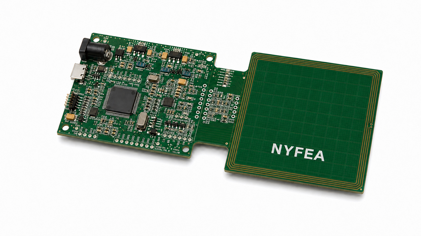
NF663 belongs on the shortlist when an engineer is designing a new multi-protocol 13.56 MHz reader or is prepared to perform a controlled hardware-and-firmware redesign. The supplied NF663 specification documents ISO/IEC 14443 A/B, JIS X 6319-4 (FeliCa scheme), ISO/IEC 15693, ISO/IEC 18092 passive-initiator operation, EPC HF modes, SPI/I²C/UART host interfaces, a 512-byte FIFO, 8 kB EEPROM, a separate SAM interface, and low-power card detection.
That functional overlap does not prove that NF663 is pin-compatible, register-compatible, firmware-compatible, or RF-network-compatible with CLRC663. Treat any CLRC663-to-NF663 change as a redesign until the exact device, board, software, antenna, and production limits pass measured validation.
How to Read the Evidence
A value or function stated in a controlled manufacturer document. Confirm the latest revision before release.
An engineering method for selection, integration, or testing. It must be adapted to the actual product.
A result that cannot be inferred from a data sheet and must be measured on production-intent hardware.
| Engineering question | Decision-ready answer |
|---|---|
| Is “CLRC663” one exact part? | No. Freeze the complete order code and silicon generation before comparing temperature range, package, features, or availability. Do not silently merge the base CLRC663 and CLRC663 plus family. |
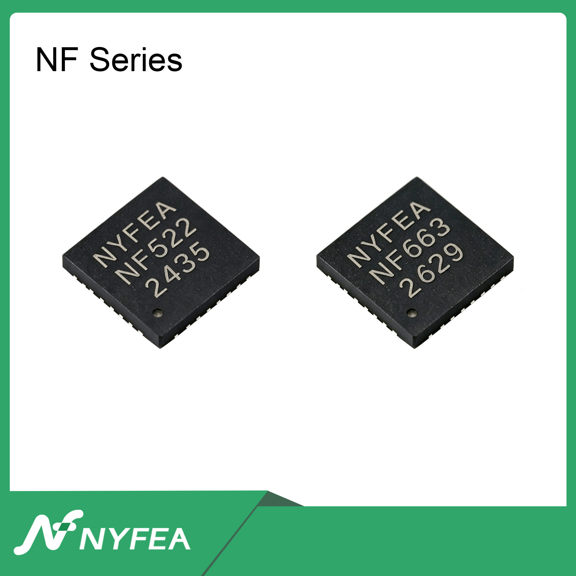
| What is NF663? | A Nyfea 13.56 MHz multi-protocol reader/writer IC in HVQFN32. It is a component, not a complete reader module. |
| Is NF663 a direct CLRC663 replacement? | No direct or drop-in claim is made in the NF663 specification supplied for this review. Use a controlled redesign and qualification process. |
| What should be compared first? | Target cards and standards, host interface, power modes, pin and supply architecture, software behavior, antenna/RF design, environmental limits, and production evidence. |
| What determines read range? | The complete RF system: antenna geometry and Q, matching, supply, credential, orientation, enclosure, nearby metal, noise, firmware settings, and compliance constraints. |
Start with the Exact CLRC663 Device, Not the Search Term
“CLRC663” is often used as a broad search label for development boards, modules, the original device, the CLRC663 plus family, and multiple ordering codes. Those are related search entities, but they are not automatically the same engineering baseline. A credible comparison begins with the full orderable part number, data-sheet revision, package, temperature grade, PCB revision, bill of materials, and firmware version.
This distinction matters because a search result for CLRC663 pinout, CLRC663 module, or CLRC663 replacement may combine information from different generations or third-party boards. For example, NXP's current CLRC663 plus product page lists an operating range up to +105 °C for the plus family; the NF663 specification reviewed for this article lists −25 °C to +85 °C. An application whose ambient or junction requirements exceed the NF663 limit cannot use keyword similarity as a selection argument.
Decision 1: Which Cards, Tags, and Protocol Roles Must Work?
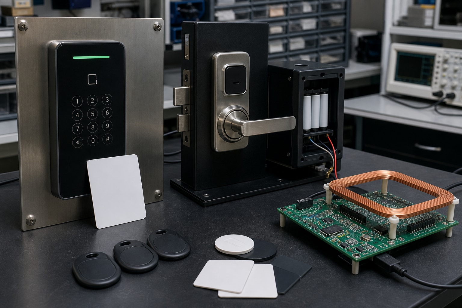
Start from the deployed credential population, not from a generic “NFC” requirement. List every card or tag family, mandatory data rate, reader role, security layer, transaction-time limit, and required interoperability corner. Two reader ICs can name the same air-interface standard while assigning different parts of anticollision, higher protocol layers, authentication, and error recovery to the host.
The NF663 specification documents reader/writer support for ISO/IEC 14443 Type A and Type B, JIS X 6319-4 (FeliCa scheme), ISO/IEC 15693, ICODE EPC UID/EPC OTP, and ISO/IEC 18000-3 Mode 3 / EPC Class-1 HF. It also documents ISO/IEC 18092 passive-initiator operation. ISO/IEC 14443 A/B rates extend to 848 kbit/s; FeliCa-scheme rates are 212 and 424 kbit/s.
Access control
Check credential families, secure authentication, transaction latency, anti-passback logic, metal door geometry, and low-power wake behavior.
Industrial identification
Check ISO/IEC 15693 tag size, orientation, read-zone control, machinery noise, cable coupling, and enclosure detuning.
Transit or ticketing
Check actual card schemes, throughput, security certification, field strength, interoperability, and application-specific approvals.
Embedded NFC devices
Check operating role, host stack responsibility, antenna volume, coexistence, update strategy, and production diagnostics.
Decision 2: What Must Change in the Host Interface and Firmware?
A reader migration is rarely defined by protocol labels alone. The engineering workload sits in reset and startup behavior, interface strapping, register semantics, command sequencing, FIFO service, interrupt handling, error recovery, EEPROM organization, timer use, and higher protocol layers.
NF663 provides SPI up to 10 Mbit/s, I²C Fast mode at 400 kBd and Fast-mode Plus at 1000 kBd, and logic-level UART up to 1228.8 kBd. It integrates a 512-byte transmit/receive FIFO and 8 kB EEPROM organized in 64-byte pages. A separate auxiliary I²C interface is intended for a secure access module. These are documented NF663 capabilities; they do not establish register-level compatibility with a CLRC663 codebase.
- Rebuild the power-on, reset, oscillator, and interface-detection sequence from controlled documents.
- Map every used register and command by behavior—not by similar name.
- Verify FIFO length, water-level interrupts, overflow handling, and host service latency.
- Exercise timeout, CRC, framing, collision, no-response, and recovery paths.
- Version configuration data and EEPROM programming so production can identify the active build.
- Treat SAM integration, key provisioning, and application security as separate system requirements.
Decision 3: What Is the Complete Power and LPCD Budget?
Low-power card detection (LPCD) is valuable only when the reader's detection margin and the complete product current are both acceptable. A microamp figure for one IC state does not include the host MCU, regulator quiescent current, wake timer, level shifting, LEDs, sensors, leakage, or antenna-related settling activity.
Under the conditions stated in its specification, NF663 lists typical values of 8 nA in power-down at 25 °C, 3 µA in standby, 3 µA during LPCD sleep, approximately 0.45 mA in modem-off, and approximately 17 mA in modem-on. NF663 uses separate VDD, PVDD, and TVDD supply functions over a documented 3.0 V to 5.5 V supply range. AVDD and DVDD are regulated outputs; they must not be treated as external supply inputs.
For an LPCD design, characterize the antenna baseline, I/Q thresholds, wake period, false-wake rate, missed-detection rate, wake-to-transaction time, and system energy per detection cycle across component, temperature, supply, enclosure, and nearby-object variations.
Decision 4: Can the Antenna and RF Path Be Revalidated?
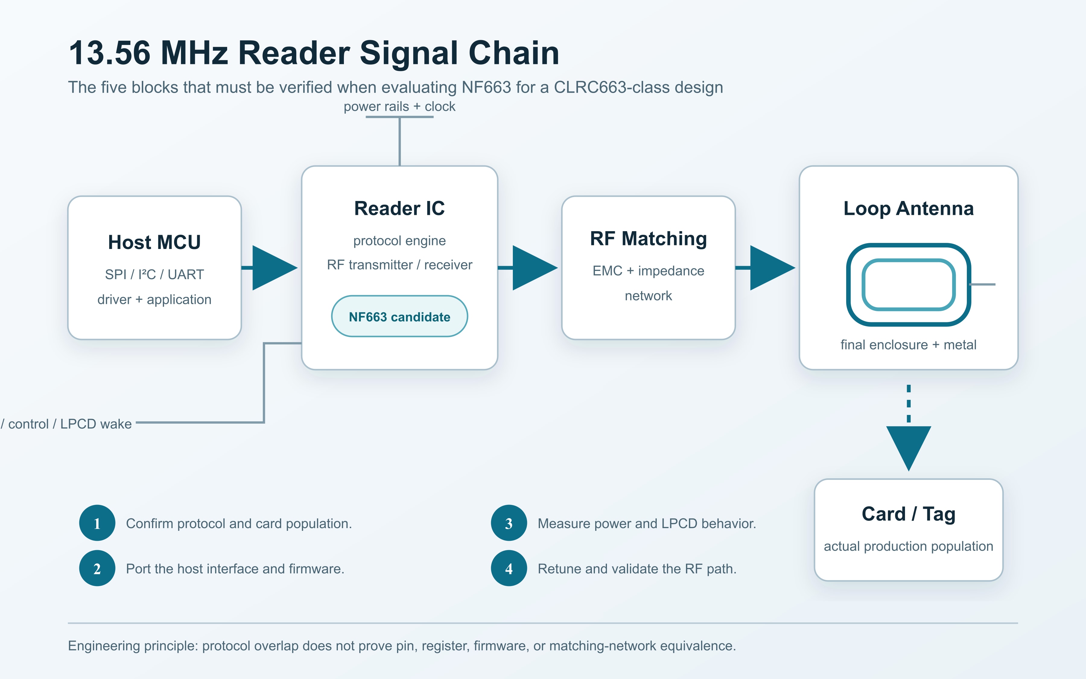
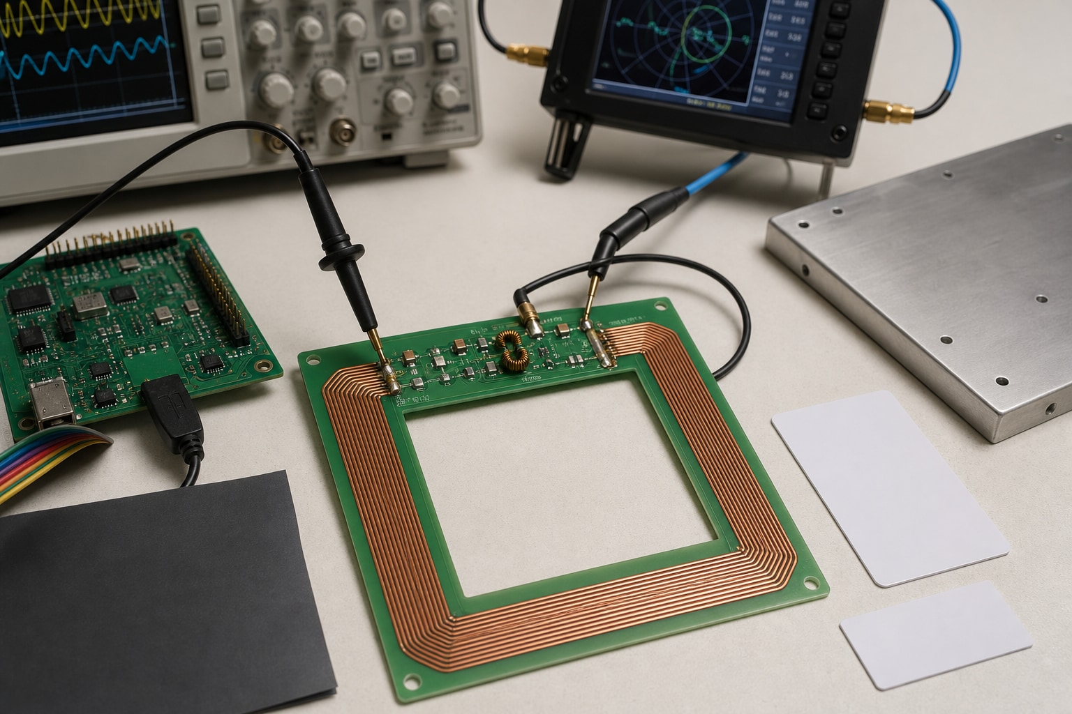
The reader IC, EMC filter, impedance-matching network, receive network, loop antenna, enclosure, nearby conductors, cable routing, supply noise, and target credential form one RF system. Component values copied from a CLRC663 evaluation board—or from any unrelated reader—are a starting hypothesis, not a production design.
NF663 uses balanced TX1/TX2 transmitter outputs and RXP/RXN receive inputs with VMID bias. Its reference topology includes EMI filtering, matching, damping, and a balanced receive path. The exact component values must be calculated and tuned from the measured antenna impedance and the product's field-strength, sensitivity, EMC, and read-zone objectives.
Decision 5: New Design, Controlled Redesign, or Drop-In Expectation?
The phrase “CLRC663 alternative” can describe three different projects. A new design is free to select a reader architecture and optimize the PCB, antenna, firmware, and qualification plan around it. A controlled redesign preserves product requirements but accepts schematic, layout, driver, RF, and validation changes. A drop-in replacement expects little or no change and therefore demands much stronger proof.
NF663 is positioned here as an independent Nyfea candidate for the first two project types. It is not presented as an NXP-endorsed replacement. The NF663 specification supplied for this review does not claim pin-to-pin, register, firmware, or RF-network compatibility with CLRC663.
Where NF663 Fits in a CLRC663-Class Design Evaluation
NF663 is most relevant when the project needs a board-level, host-controlled, multi-protocol 13.56 MHz reader with a substantial FIFO, nonvolatile configuration storage, multiple host interfaces, optional SAM connectivity, and LPCD. It is less suitable when the project requires an environmental grade outside its documented limits, demands a certified drop-in replacement, or cannot allocate engineering time for driver porting and RF requalification.
| NF663 documented capability | What it enables | What the project still must prove |
|---|---|---|
| ISO/IEC 14443 A/B; FeliCa scheme; ISO/IEC 15693; ISO/IEC 18092 passive initiator; EPC HF modes | One reader candidate for several proximity, vicinity, and HF tag populations | Actual credential interoperability, host protocol layers, security, timing, and approvals |
| SPI, I²C, and UART host interfaces | Architectural choice for different MCU platforms | Pin strapping, logic levels, signal integrity, startup, driver behavior, and recovery |
| 512-byte FIFO and 8 kB EEPROM | Buffered transfers and nonvolatile configuration resources | Interrupt latency, overflow handling, data integrity, access control, and production programming |
| Power-down, standby, modem-off, and LPCD | Low-duty-cycle reader operation | Total product current, detection margin, false wakes, missed cards, and wake time |
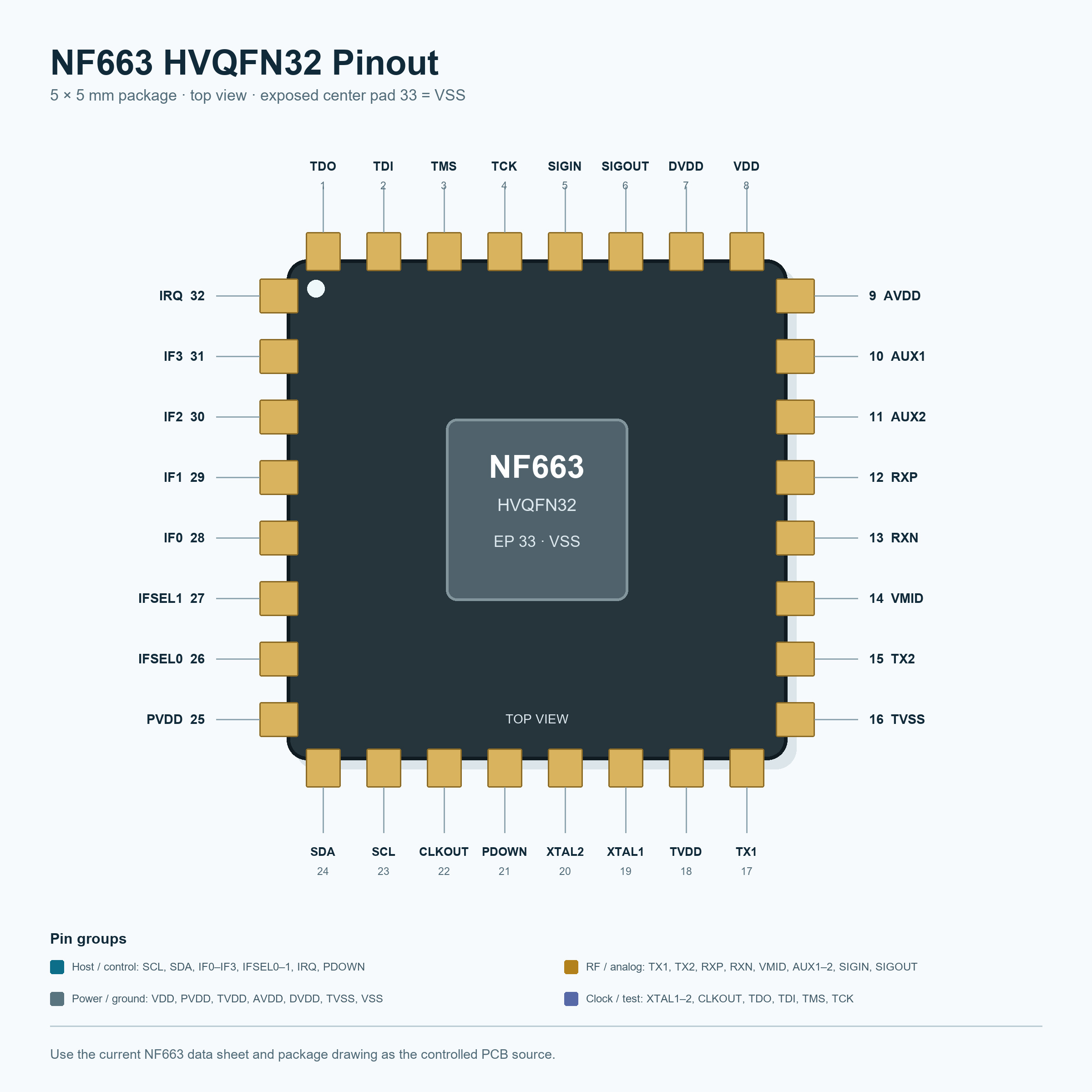
| HVQFN32, 5 mm × 5 mm nominal body | Compact board-level implementation | Land pattern, exposed-pad grounding, assembly yield, inspection, thermal and EMC performance |
NF663 vs CLRC663: Use a Verified Comparison Boundary
A responsible comparison separates public family-level overlap from project-specific equivalence. The table below is intentionally conservative: it identifies the engineering question and the evidence required rather than asserting unverified one-to-one behavior.
| Comparison area | Publicly visible overlap | Required migration evidence |
|---|---|---|
| Operating concept | Both are associated with host-controlled, multi-protocol 13.56 MHz reader/front-end designs. | Exact operating roles, protocol layers, commands, timing, error behavior, and card-set results. |
| Contactless technologies | Family-level references include major 13.56 MHz proximity, vicinity, FeliCa-scheme, and related modes. | Compare the exact CLRC663 order code and current documents line by line against NF663 requirements. |
| Host connection | SPI, I²C, and UART are relevant interface categories. | Pin multiplexing, voltage domains, bus timing, framing, reset behavior, IRQ handling, and firmware driver port. |
| Package class | HVQFN32 is relevant to the compared product class. | Never infer footprint compatibility. Compare every pin, exposed pad, mechanical tolerance, land pattern, and assembly rule. |
| Low-power operation | Low-power card detection is a selection topic for both design contexts. | State definitions, test conditions, antenna baseline, thresholds, false-wake behavior, and complete-system current. |
| RF interface | Both require an external matching network and antenna in a complete reader. | Topology, component stress, transmitter settings, receiver network, antenna impedance, tuning, EMC, and final read zone. |
| Environmental limits | Both have published operating limits tied to specific devices. | NF663: −25 °C to +85 °C in the reviewed specification. Confirm the exact CLRC663 grade and all product-level thermal requirements. |
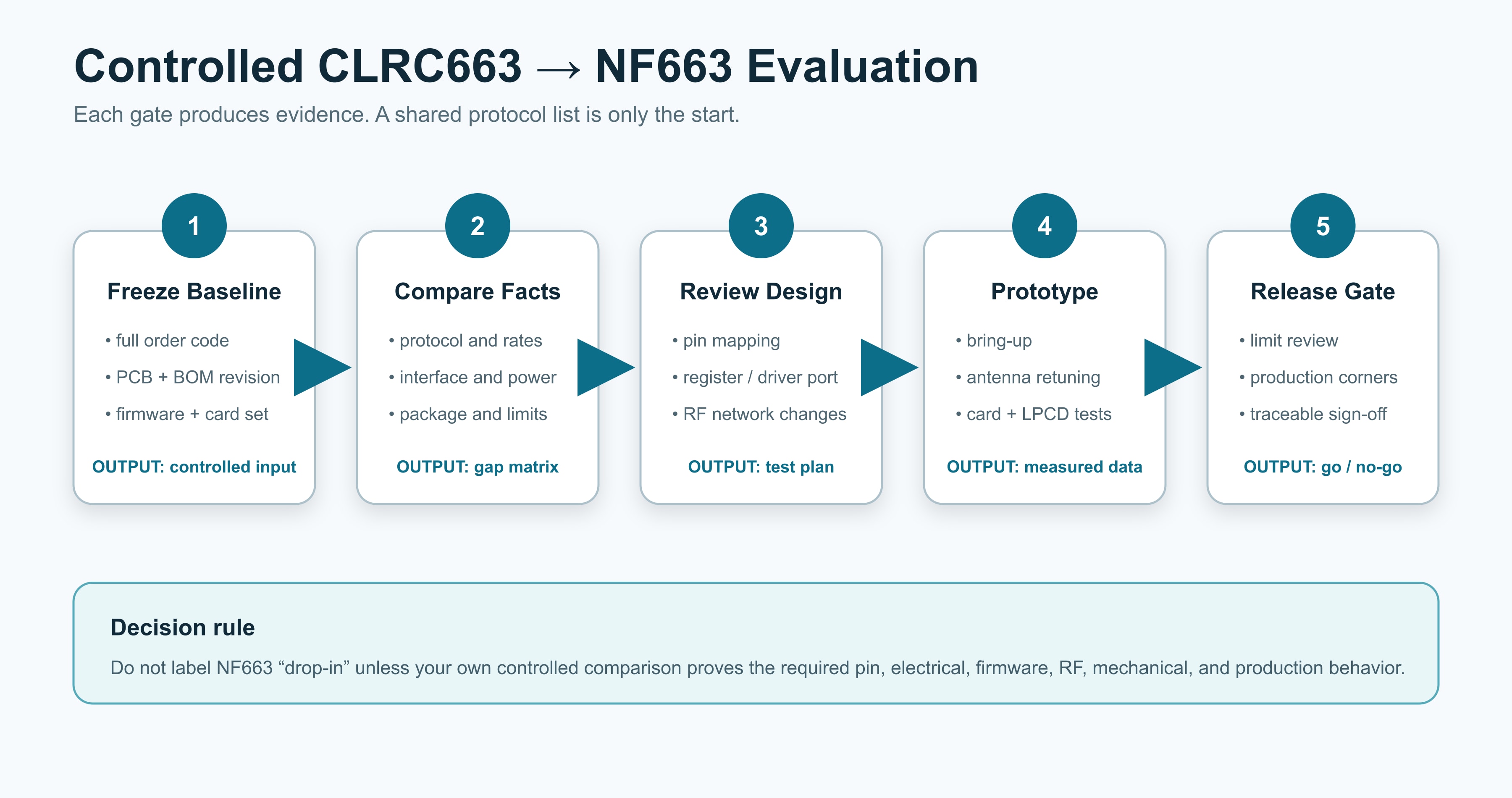
A Controlled CLRC663-to-NF663 Evaluation Workflow
- Freeze the baseline. Capture the complete CLRC663 order code, schematics, PCB and BOM revision, antenna drawing, firmware build, register configuration, card/tag population, measured range, current, transaction time, and known failure cases.
- Create a traceable gap matrix. Compare protocols and roles, rates, pinout, voltage domains, absolute limits, clocks, interfaces, registers, commands, FIFO, EEPROM, timers, interrupts, LPCD, RF pins, package, and qualification evidence.
- Define acceptance limits before prototyping. Include interoperability, range distribution, orientation, current by state, wake response, error recovery, temperature and supply corners, EMC, ESD, and manufacturing tolerances.
- Build an NF663 prototype around the NF663 reference requirements. Do not force an inherited CLRC663 footprint or RF network unless the comparison independently proves every relevant detail.
- Bring up by layer. Verify rails and clock, then host communication, command/IRQ/FIFO behavior, RF field and receive path, protocol operation, LPCD, and fault recovery.
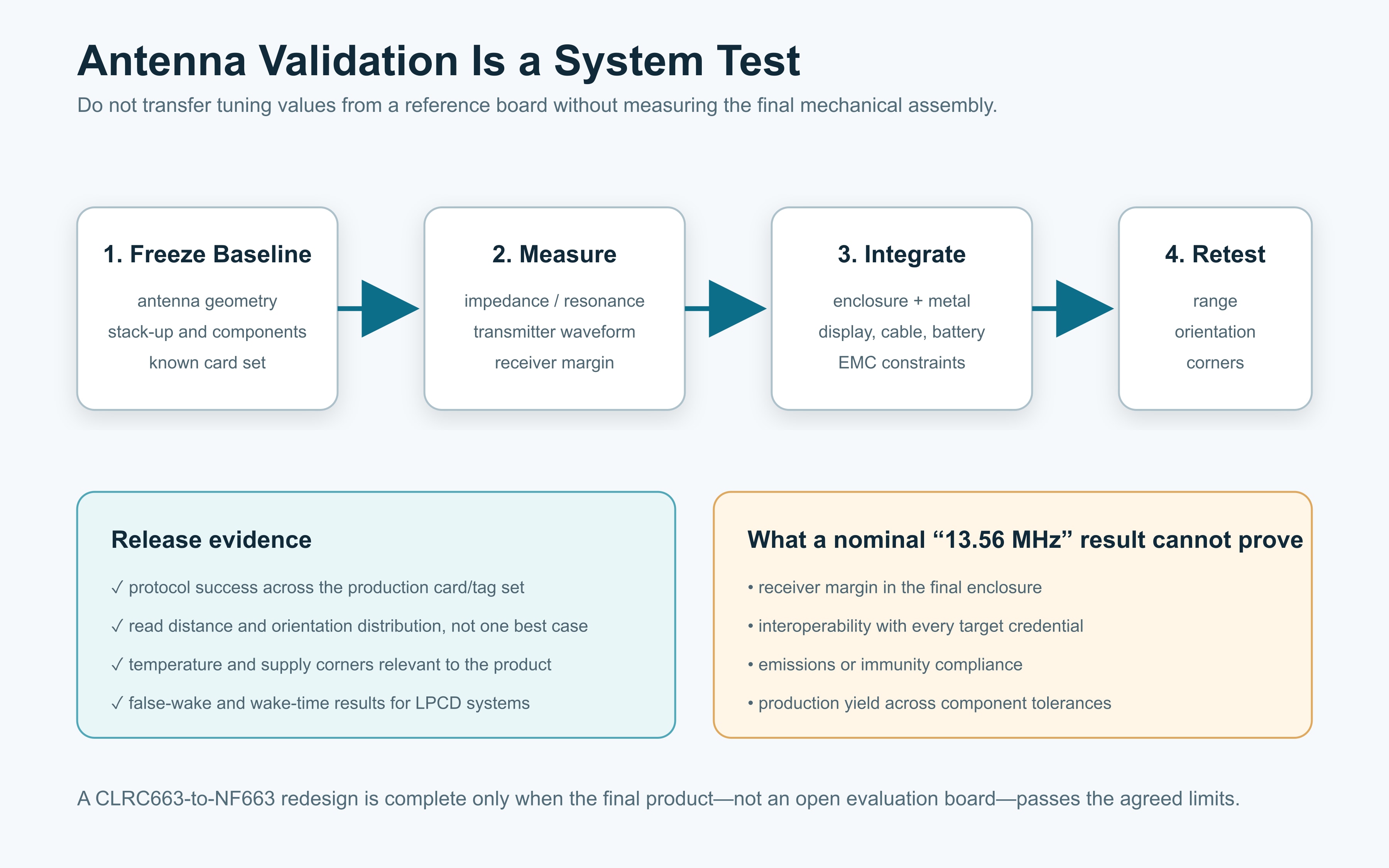
- Retune in final mechanics. Measure the assembled product with its real enclosure, metal, cable, display, battery, and credential population.
- Release from evidence. Record test conditions, raw results, limit review, deviations, production programming, and sign-off. Keep supplier and revision traceability.
Evidence Required Before Production Release
- Traceability: exact IC ordering code, lot controls, data-sheet revision, PCBA revision, BOM, firmware, configuration data, and test fixture version.
- Electrical: all rails, ramp/reset behavior, clock startup, host timing, pin stress, current in every state, thermal margin, and fault recovery.
- RF: antenna impedance, matching tolerance, transmitter waveform, receiver margin, field distribution, read-zone limits, detuning, and EMC pre-compliance.
- Interoperability: production-representative cards/tags, orientations, distances, transaction types, collision cases, damaged or weak credentials, and repeated cycles.
- LPCD: sleep current, detection probability, false-wake rate, wake latency, baseline recalibration, and nearby-object sensitivity.
- Environment and manufacturing: temperature, supply corners, component tolerances, enclosure variants, ESD/immunity, assembly yield, programming, and end-of-line test limits.
- Compliance and security: product-specific approvals, key management, secure boot/update policy, vulnerability review, and market obligations.
A data sheet supports component selection; it does not certify the complete reader. Read range, payment or transit suitability, access-control security, EMV performance, regulatory compliance, and production reliability belong to the final product and its evidence package.
CLRC663 and NF663 Engineering FAQs
What is CLRC663 used for?
CLRC663 is associated with high-performance, host-controlled, multi-protocol 13.56 MHz NFC/HF reader frontends. Search intent commonly includes access control, industrial identification, ticketing, embedded readers, development boards, antenna design, pinout, LPCD, and replacement evaluation. The exact capability depends on the full device and controlled NXP documentation.
Is NF663 a CLRC663 alternative?
NF663 can be considered as an independent candidate for a new or redesigned multi-protocol 13.56 MHz reader. The reviewed NF663 specification does not claim drop-in compatibility with CLRC663, so the correct process is a documented gap analysis followed by prototype and system validation.
Can NF663 directly replace CLRC663 on an existing PCB?
Do not assume it can. Compare every pin, exposed-pad connection, supply domain, clock, interface selection, electrical limit, package tolerance, register, command, firmware function, RF network, and production requirement. Until these are proven, plan for schematic, PCB, driver, and antenna changes.
Which protocols does NF663 support?
The supplied NF663 specification documents ISO/IEC 14443 Type A/B reader/writer, JIS X 6319-4 (FeliCa scheme), ISO/IEC 15693, ISO/IEC 18092 passive initiator, ICODE EPC UID/EPC OTP, and ISO/IEC 18000-3 Mode 3 / EPC Class-1 HF operation. Confirm application-layer and security responsibilities in the host.
What host interfaces are available on NF663?
NF663 documents SPI up to 10 Mbit/s, I²C Fast mode at 400 kBd and Fast-mode Plus at 1000 kBd, and logic-level UART up to 1228.8 kBd. It also provides a separate auxiliary I²C connection for a secure access module.
What read range can NF663 achieve?
The specification states a typical maximum of up to 12 cm with an ISO/IEC 14443 Type A or MIFARE card depending on antenna size and tuning. This is not a guaranteed product range. Measure the actual antenna, credential, orientation, enclosure, supply, interference, and firmware configuration.
Does NF663 support low-power card detection?
Yes. NF663 documents LPCD together with standby, power-down, and modem-off modes. Product design still requires complete-system current measurement and validation of detection margin, false wakes, missed cards, and wake time under real environmental and mechanical conditions.
Can a CLRC663 antenna network be reused for NF663?
Do not copy the values without analysis and measurement. Use the NF663 reference topology and limits, measure the actual antenna impedance, calculate the filter and matching network, and validate the final product for transmitter waveform, receiver margin, read zone, EMC, temperature, and tolerance.
Is NF663 a complete NFC reader module?
No. NF663 is a board-level reader/writer IC. A complete reader also needs a host MCU, power circuitry, 27.12 MHz clock implementation, RF filtering and matching, antenna, firmware, mechanical integration, validation, and applicable approvals.
Controlled Sources and Design Authority
- NXP — CLRC663 plus family product page. Use the exact order-code data sheet and current revision for CLRC663 design decisions.
- NXP — CLRC663 high-performance multi-protocol NFC frontend. Confirm lifecycle and document applicability for the selected device.
- Nyfea — NF663 multi-protocol 13.56 MHz RFID reader IC. Product overview and access to the controlled NF663 product specification.
The linked manufacturer documents—not this article or its explanatory graphics—are the component design authority. End-product performance and compliance must be established by the product owner through appropriate engineering and qualification.
Evaluate NF663 Against Your Actual Reader Requirements
Send Nyfea your target cards and tags, host interface, antenna dimensions, supply architecture, operating temperature, LPCD target, current CLRC663 order code, and production constraints. The useful next step is a traceable gap review—not a generic replacement claim.
CLRC663, MIFARE, NXP, FeliCa, ICODE, and related product names or marks belong to their respective owners. NF663 is a Nyfea product. Nyfea and NF663 are not affiliated with, endorsed by, or sponsored by NXP. References to third-party products are used only to define engineering search context and evaluation boundaries.